参数资料
| 型号: | AD6654BBC |
| 厂商: | Analog Devices Inc |
| 文件页数: | 84/88页 |
| 文件大小: | 0K |
| 描述: | IC ADC 14BIT W/6CH RSP 256CSPBGA |
| 标准包装: | 1 |
| 位数: | 14 |
| 采样率(每秒): | 92.16M |
| 数据接口: | 串行,并联 |
| 转换器数目: | 1 |
| 功率耗散(最大): | 2.5W |
| 电压电源: | 模拟和数字 |
| 工作温度: | -25°C ~ 85°C |
| 安装类型: | 表面贴装 |
| 封装/外壳: | 256-BGA,CSPBGA |
| 供应商设备封装: | 256-CSPBGA(17x17) |
| 包装: | 托盘 |
| 输入数目和类型: | 1 个差分,单极 |
第1页第2页第3页第4页第5页第6页第7页第8页第9页第10页第11页第12页第13页第14页第15页第16页第17页第18页第19页第20页第21页第22页第23页第24页第25页第26页第27页第28页第29页第30页第31页第32页第33页第34页第35页第36页第37页第38页第39页第40页第41页第42页第43页第44页第45页第46页第47页第48页第49页第50页第51页第52页第53页第54页第55页第56页第57页第58页第59页第60页第61页第62页第63页第64页第65页第66页第67页第68页第69页第70页第71页第72页第73页第74页第75页第76页第77页第78页第79页第80页第81页第82页第83页当前第84页第85页第86页第87页第88页
AD6654
Rev. 0 | Page 85 of 88
DDC DESIGN NOTES
The following guidelines describe circuit connections, layout
requirements, and programming procedures for the AD6654.
The designer should review these guidelines before starting the
system design and layout.
The AD6654 requires the following power-up sequence.
The VDDCORE (1.8 V) is required to settle into nominal
voltage levels before the VDDIO attains the minimum.
The DDC input clock (CLK) and input (EXP) pins EXP[2:0]
are not 5 V tolerant. Care should be taken to drive these
pins within the limits of VDDIO (3.0 V to 3.6 V). This is
easily accomplished by using the ADC data ready (DR)
output to drive the DDC clock (CLK) input.
The number format used in this part is twos complement.
All input ports and output ports use twos complement data
format. The formats for individual internal registers are
given in the memory map description of these registers.
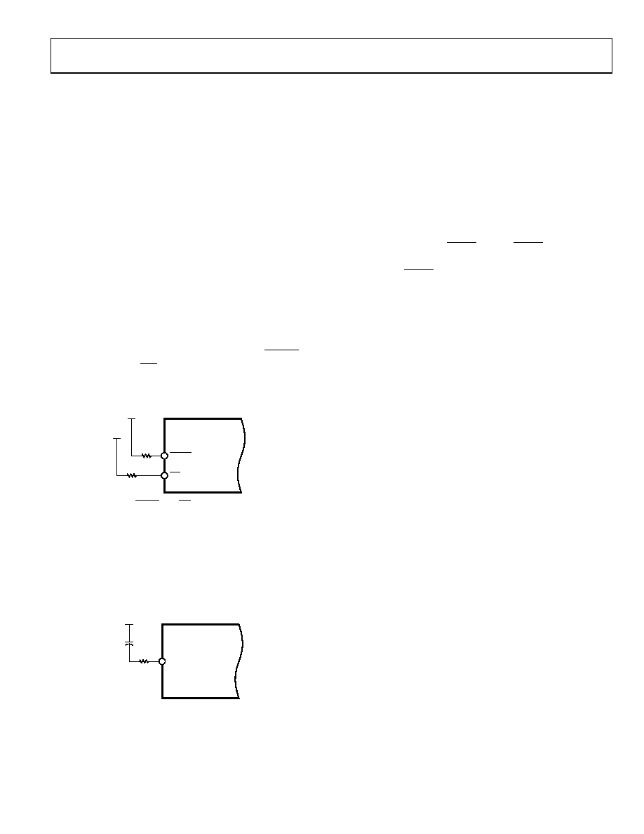
In both microport and serial port operation, the DTACK
(RDY, SDO) and IRP pins are open-drain outputs and
should be terminated externally to VDDIO through a 1 kΩ
pull-up resistor.
05156-056
DTACK (RDY, SDO)
AD6654
1k
3.3V
1k
3.3V
IRP
Figure 75. DTACK, SDO, IRP Pull-Up Resistor Circuit
A simple RC circuit is used on the EXT_FILTER pin to
balance the internal RC circuit on this pin and maintain a
good PLL clock lock. The recommended circuit is given in
Figure 76. It is further recommended that this RC circuit be
placed as close as possible to the AD6654 part. This layout
consideration ensures that the PLL clock is clean and the
PLL lock is closely maintained.
05156-057
EXT_FILTER
AD6654
250
VDD CORE
0.01
F
Figure 76. EXT_FILTER Circuit for PLL Clock
By default, the PLL CLK is disabled. It can be enabled by
programming the PLL multiplier and divider bits in the
ADC CLK control register. When the PLL CLK is enabled
by programming this register, it takes about 50 s to 200 s
to settle down. While the PLL loop settles down, the voltage
at the EXT_FILTER pin increases from 0 V to VDDCORE
(1.8 V) and settles there. Channel registers and output port
registers (Address 0x68 to Address 0xE7) should not be pro-
grammed before the PLL loop settles down.
To reset the AD6654, the user must provide a minimum
pulse of 30 ns to the RESET pin. The RESET pin should be
connected to GND (or pulled low) during power-up of the
part. The RESET pin can be pulled high after the power
supplies have settled to nominal values (1.8 V and
3.3 V). At this point, a pulse (pull low and high again)
should be provided to give a reset to the part.
The CPUCLK (SCLK) is the clock used for programming
via the microport (serial port). This clock needs to be
provided by the designer to the part (slave clock). The
designer should ensure that this clock’s frequency is less
than or equal to the frequency of the CLK signal. Addi-
tionally, the frequency of the CPUCLK (SCLK) should
always be less than 100 MHz.
The microport data bus is 16 bits wide. Both 8-bit and
16-bit modes are available using this part. If 8-bit mode is
used, the MSB of the data bus (D[15:8]) can be left floating
or connected to GND.
The output parallel port has a 1-clock cycle overhead. If two
channels (with the same data rates) are output on one
output port in 16-bit interleaved I/Q mode along with an
AGC word, this requires three clock cycles for one sample
from each channel (one clock each for I data, Q data, and
gain data). Therefore, the total number of clock cycles
required to output the data is 3 clocks/channel × 2 channels
+ 1 (overhead) = 7 clock cycles. The number of clock cycles
required for each channel can be 3 (interleaved I + Q + gain
word), or 2 (parallel I /Q + gain) or 2 (interleaved I + Q) or
1 (interleaved I/Q). Designers should make sure that suffi-
cient time is allowed to output these channels on one output
port. Also note that the I, Q, and gain for a particular
channel come out on a single output port and cannot be
divided among output ports.
When CRCF and DRCF filters are disabled, the coefficient
memory cannot be read back, because the clock to the
coefficient RAM is also cut off.
相关PDF资料 |
PDF描述 |
|---|---|
| AD670KNZ | IC ADC 8BIT SGNL COND 20DIP |
| AD673JNZ | IC ADC 8BIT REF/CLK/COMP 20DIP |
| AD674BJN | IC ADC 12BIT MONO 3OUT 28-DIP |
| AD676BD | IC ADC 16BIT SAMPLING 28-CDIP |
| AD677BD | IC ADC 16BIT SAMPLING 16-CDIP |
相关代理商/技术参数 |
参数描述 |
|---|---|
| AD6654BBCZ | 功能描述:IC ADC 14BIT W/6CH RSP 256CSPBGA RoHS:是 类别:集成电路 (IC) >> 数据采集 - 模数转换器 系列:- 产品培训模块:Lead (SnPb) Finish for COTS Obsolescence Mitigation Program 标准包装:250 系列:- 位数:12 采样率(每秒):1.8M 数据接口:并联 转换器数目:1 功率耗散(最大):1.82W 电压电源:模拟和数字 工作温度:-40°C ~ 85°C 安装类型:表面贴装 封装/外壳:48-LQFP 供应商设备封装:48-LQFP(7x7) 包装:管件 输入数目和类型:2 个单端,单极 |
| AD6654CBC | 功能描述:IC ADC 14BIT W/4CH RSP 256CSPBGA RoHS:否 类别:集成电路 (IC) >> 数据采集 - 模数转换器 系列:- 产品培训模块:Lead (SnPb) Finish for COTS Obsolescence Mitigation Program 标准包装:250 系列:- 位数:12 采样率(每秒):1.8M 数据接口:并联 转换器数目:1 功率耗散(最大):1.82W 电压电源:模拟和数字 工作温度:-40°C ~ 85°C 安装类型:表面贴装 封装/外壳:48-LQFP 供应商设备封装:48-LQFP(7x7) 包装:管件 输入数目和类型:2 个单端,单极 |
| AD6654CBCZ | 功能描述:IC ADC 14BIT W/4CH RSP 256CSPBGA RoHS:是 类别:集成电路 (IC) >> 数据采集 - 模数转换器 系列:- 产品培训模块:Lead (SnPb) Finish for COTS Obsolescence Mitigation Program 标准包装:250 系列:- 位数:12 采样率(每秒):1.8M 数据接口:并联 转换器数目:1 功率耗散(最大):1.82W 电压电源:模拟和数字 工作温度:-40°C ~ 85°C 安装类型:表面贴装 封装/外壳:48-LQFP 供应商设备封装:48-LQFP(7x7) 包装:管件 输入数目和类型:2 个单端,单极 |
| AD6654XBCZ | 制造商:Analog Devices 功能描述:14-BIT, 92.16 MSPS, 4 & 6-CHANNEL WIDEBAND IF TO BASE BAND R - Bulk |
| AD6655 | 制造商:AD 制造商全称:Analog Devices 功能描述:IF Diversity Receiver |
发布紧急采购,3分钟左右您将得到回复。