- 您现在的位置:买卖IC网 > PDF目录16836 > AD9549A/PCBZ (Analog Devices Inc)BOARD EVALUATION FOR AD9549A PDF资料下载
参数资料
| 型号: | AD9549A/PCBZ |
| 厂商: | Analog Devices Inc |
| 文件页数: | 33/76页 |
| 文件大小: | 0K |
| 描述: | BOARD EVALUATION FOR AD9549A |
| 设计资源: | AD9549 Schematics AD9549 Gerber Files |
| 标准包装: | 1 |
| 主要目的: | 计时,时钟发生器 |
| 嵌入式: | 否 |
| 已用 IC / 零件: | AD9549A |
| 主要属性: | 8 kHz ~ 750 MHz 输入 |
| 次要属性: | 差分输出 |
| 已供物品: | 板 |
第1页第2页第3页第4页第5页第6页第7页第8页第9页第10页第11页第12页第13页第14页第15页第16页第17页第18页第19页第20页第21页第22页第23页第24页第25页第26页第27页第28页第29页第30页第31页第32页当前第33页第34页第35页第36页第37页第38页第39页第40页第41页第42页第43页第44页第45页第46页第47页第48页第49页第50页第51页第52页第53页第54页第55页第56页第57页第58页第59页第60页第61页第62页第63页第64页第65页第66页第67页第68页第69页第70页第71页第72页第73页第74页第75页第76页
AD9549
Rev. D | Page 39 of 76
06744-
049
1
0
1
0
1
0
REFAB LOR
REFAB OOL
REFAB INVALID
REFAB
PHASE LOCK
FREQUENCY LOCK
IRQ
REF INVALID
PHASE LOCK
FREQ. LOCK
REF LOR
REF OOL
IRQ
STATUS PIN
(1 OF 4)
STATUS PIN
CONTROL REGISTER
(1 OF 4)
REFA LOR
REFA OOL
REFA INVALID
REFB LOR
REFB OOL
REFB INVALID
PHASE LOCK DETECT
FREQUENCY LOCK DETECT
IRQ
INTERNAL
STATUS FLAGS
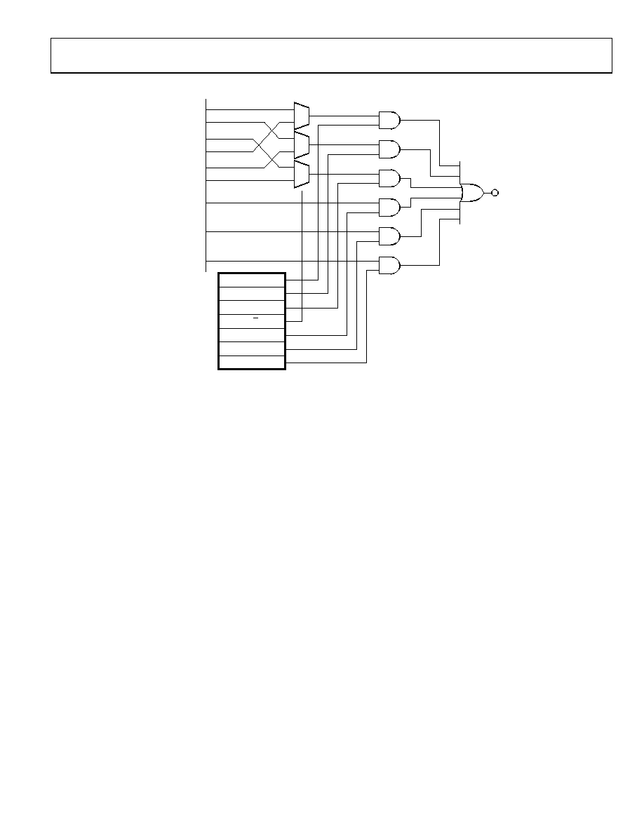
Figure 49. Status Pin Control
STATUS AND WARNINGS
Status Pins
Four pins (S1 to S4) are reserved for providing device status
information to the external environment. These four pins are
individually programmable (via the serial I/O port) as an OR'ed
combination of six possible status indications. Each pin has a
dedicated group of control register bits that determine which
internal status flags are used to provide an indication on a
particular pin, as shown in Figure 49.
Reference Monitor Status
In the case of reference monitoring status information, a pin
can be programmed for either REFA or REFB, but not both.
In addition, the OR'ed output configuration allows the user to
combine multiple status flags into a single status indication. For
example, if both the LOR and OOL control register bits are true,
the status pin associated with that particular control register
gives an indication if either the LOR or OOL status flag is
asserted for the selected reference (A or B).
Default DDS Output Frequency on Power-Up
The four status pins (S1 to S4) provide a completely separate
function at power-up. They can be used to define the output
frequency of the DDS at power-up even though the I/O registers
have not yet been programmed. This is made possible because
the status pins are designed with bidirectional drivers. At power-
up, internal logic initiates a reset pulse of about 10 ns. During
this time, S1 to S4 briefly function as input pins and can be
driven externally. Any logic levels thus applied are transferred
to a 4-bit register on the falling edge of the internally initiated
pulse. The falling edge of the pulse also returns S1 to S4 to their
normal function as output pins. The same behavior occurs
when the RESET pin is asserted manually.
Setting up S1 to S4 for default DDS start-up is accomplished by
connecting a resistor to each pin (either pull-up or pull-down)
to produce the desired bit pattern, yielding 16 possible states
that are used both to address an internal 8 × 16 ROM and to
select the SYSCLK mode (see Table 8). The ROM contains eight
16-bit DDS frequency tuning words (FTWs), one of which is
selected by the state of the S1 to S3 pins. The selected FTW is
transferred to the FTW0 register in the I/O register map without
the need for an I/O update. This ensures that the DDS generates
the selected frequency even if the I/O registers have not been
programmed. The state of the S4 pin selects whether the internal
system clock is generated by means of the internal SYSCLK PLL
multiplier or not (see the SYSCLK Inputs section for details).
相关PDF资料 |
PDF描述 |
|---|---|
| ESC05DRTS-S734 | CONN EDGECARD 10POS DIP .100 SLD |
| MAX6250BEPA+ | IC VREF SERIES BURIED ZNR 8-PDIP |
| MAX6133A30+T | IC VREF SERIES PREC 3V 8-UMAX |
| MAX6133A41+T | IC VREF SERIES PREC 4.096V 8UMAX |
| MAX6133A50+T | IC VREF SERIES PREC 5V 8-UMAX |
相关代理商/技术参数 |
参数描述 |
|---|---|
| AD9549BCPZ | 制造商:Analog Devices 功能描述: |
| AD9549BCPZ-REEL7 | 制造商:Analog Devices 功能描述:PLL CLOCK SYNTHESIZER SGL 64LFCSP EP - Tape and Reel |
| AD9549BCPZ-TR | 制造商:Analog Devices 功能描述:650MHZ DDS CLK GEN W/SYNCH REEL - Tape and Reel |
| AD9549XCPZ | 制造商:AD 制造商全称:Analog Devices 功能描述:Dual Input Network Clock Generator/Synchronizer |
| AD9550 | 制造商:AD 制造商全称:Analog Devices 功能描述:Integer-N Clock Translator for Wireline Communications |
发布紧急采购,3分钟左右您将得到回复。