- 您现在的位置:买卖IC网 > PDF目录16836 > AD9549A/PCBZ (Analog Devices Inc)BOARD EVALUATION FOR AD9549A PDF资料下载
参数资料
| 型号: | AD9549A/PCBZ |
| 厂商: | Analog Devices Inc |
| 文件页数: | 9/76页 |
| 文件大小: | 0K |
| 描述: | BOARD EVALUATION FOR AD9549A |
| 设计资源: | AD9549 Schematics AD9549 Gerber Files |
| 标准包装: | 1 |
| 主要目的: | 计时,时钟发生器 |
| 嵌入式: | 否 |
| 已用 IC / 零件: | AD9549A |
| 主要属性: | 8 kHz ~ 750 MHz 输入 |
| 次要属性: | 差分输出 |
| 已供物品: | 板 |
第1页第2页第3页第4页第5页第6页第7页第8页当前第9页第10页第11页第12页第13页第14页第15页第16页第17页第18页第19页第20页第21页第22页第23页第24页第25页第26页第27页第28页第29页第30页第31页第32页第33页第34页第35页第36页第37页第38页第39页第40页第41页第42页第43页第44页第45页第46页第47页第48页第49页第50页第51页第52页第53页第54页第55页第56页第57页第58页第59页第60页第61页第62页第63页第64页第65页第66页第67页第68页第69页第70页第71页第72页第73页第74页第75页第76页
AD9549
Rev. D | Page 17 of 76
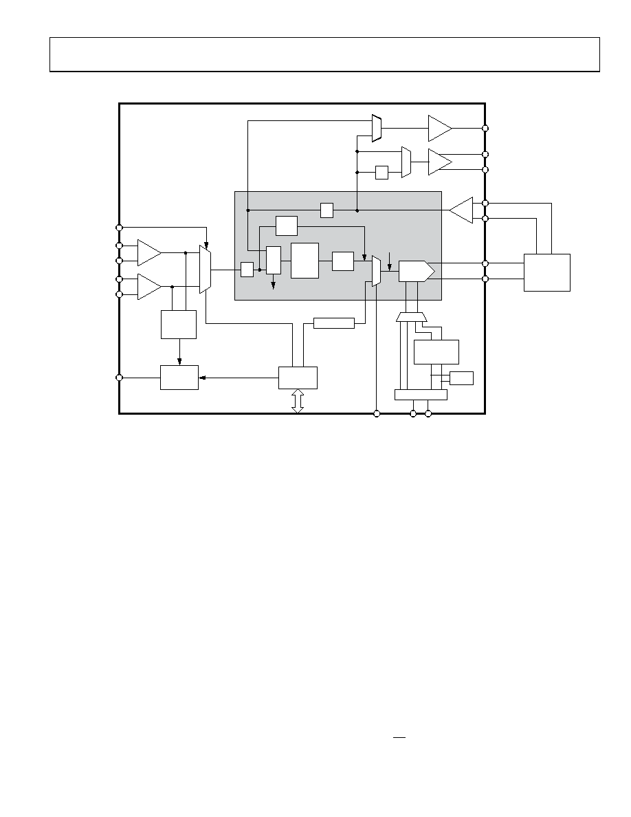
THEORY OF OPERATION
06744-
022
DDS/DAC
FREQUENCY
TUNING
WORD
SLEW
LIMIT
PROG.
DIGITAL
LOOP
FILTER
PFD
÷R
FREQ
EST.
÷S
LOCK DETECT
2×
DIGITAL PLL CORE
HOLDOVER
CONTROL
LOGIC
LOW NOISE
CLOCK
MULTIPLIER
SYSCLK PORT
INPUT
REF
MONITOR
IRQ AND
STATUS
LOGIC
OOL AND LOR
REF_CNTRL
EXTERNAL
ANALOG
LOW-PASS
FILTER
DIGITAL
INTERFACE
HOLDOVER
SYSCLK
FDBK_IN
DAC_OUT
OUT
OUT_CMOS
S1 TO S4
REFB_IN
REFA_IN
REFSELECT
AMP
Figure 22. Detailed Block Diagram
OVERVIEW
The AD9549 provides a clocking output that is directly related
in phase and frequency to the selected (active) reference (REFA
or REFB) but has a phase noise spectrum primarily governed
by the system clock. A wide band of reference frequencies is
supported. Jitter existing on the active reference is greatly reduced
by a programmable digital filter in the digital phase-locked loop
(PLL), which is the core of this product. The AD9549 supports
both manual and automatic holdover. While in holdover, the
AD9549 continues to provide an output as long as the system
clock is maintained. The frequency of the output during hold-
over is an average of the steady state output frequency prior to
holdover.
Also offered are manual and automatic switchover modes for
changing between the two references, should one become suspect
or lost. A digitally controlled oscillator (DCO) is implemented
using a direct digital synthesizer (DDS) with an integrated output
digital-to-analog converter (DAC), clocked by the system clock.
A bypassable PLL-based frequency multiplier is present, enabling
use of an inexpensive, low frequency source for the system clock.
For best jitter performance, the system clock PLL should be
bypassed; and a low noise, high frequency system clock should be
provided directly. Sampling theory sets an upper bound for the
DDS output frequency at 50%
of fS (where fS is the DAC sample rate), but a practical limitation
of 40% of fS is generally recommended to allow for the selectivity
of the required off-chip reconstruction filter. The output signal
from the reconstruction filter is fed back to the AD9549, both
to complete the PLL and to be processed through the output
circuitry. The output circuitry includes HSTL and CMOS output
buffers, as well as a frequency doubler for designs that must
provide frequencies above the Nyquist level of the DDS.
The individual functional blocks are described in the following
sections.
DIGITAL PLL CORE (DPLLC)
The digital phase-locked loop core (DPLLC) includes the
frequency estimation block and the digital phase lock control
block driving the DDS.
The start of the DPLLC signal chain is the reference signal, fR,
which appears on REFA or REFB inputs. The frequency of this
signal can be divided by an integer factor of R via the feedforward
divider. The output of the feedforward divider is routed to the
phase/frequency detector (PFD). Therefore, the frequency at
the input to the PFD is given by
R
f
R
PFD =
相关PDF资料 |
PDF描述 |
|---|---|
| ESC05DRTS-S734 | CONN EDGECARD 10POS DIP .100 SLD |
| MAX6250BEPA+ | IC VREF SERIES BURIED ZNR 8-PDIP |
| MAX6133A30+T | IC VREF SERIES PREC 3V 8-UMAX |
| MAX6133A41+T | IC VREF SERIES PREC 4.096V 8UMAX |
| MAX6133A50+T | IC VREF SERIES PREC 5V 8-UMAX |
相关代理商/技术参数 |
参数描述 |
|---|---|
| AD9549BCPZ | 制造商:Analog Devices 功能描述: |
| AD9549BCPZ-REEL7 | 制造商:Analog Devices 功能描述:PLL CLOCK SYNTHESIZER SGL 64LFCSP EP - Tape and Reel |
| AD9549BCPZ-TR | 制造商:Analog Devices 功能描述:650MHZ DDS CLK GEN W/SYNCH REEL - Tape and Reel |
| AD9549XCPZ | 制造商:AD 制造商全称:Analog Devices 功能描述:Dual Input Network Clock Generator/Synchronizer |
| AD9550 | 制造商:AD 制造商全称:Analog Devices 功能描述:Integer-N Clock Translator for Wireline Communications |
发布紧急采购,3分钟左右您将得到回复。