- 您现在的位置:买卖IC网 > PDF目录1900 > ADUC7021BCPZ62-RL7 (Analog Devices Inc)IC MCU 12BIT 1MSPS UART 40-LFCSP PDF资料下载
参数资料
| 型号: | ADUC7021BCPZ62-RL7 |
| 厂商: | Analog Devices Inc |
| 文件页数: | 36/92页 |
| 文件大小: | 0K |
| 描述: | IC MCU 12BIT 1MSPS UART 40-LFCSP |
| 标准包装: | 750 |
| 系列: | MicroConverter® ADuC7xxx |
| 核心处理器: | ARM7 |
| 芯体尺寸: | 16/32-位 |
| 速度: | 44MHz |
| 连通性: | EBI/EMI,I²C,SPI,UART/USART |
| 外围设备: | PLA,PWM,PSM,温度传感器,WDT |
| 输入/输出数: | 13 |
| 程序存储器容量: | 64KB(32K x 16) |
| 程序存储器类型: | 闪存 |
| RAM 容量: | 2K x 32 |
| 电压 - 电源 (Vcc/Vdd): | 2.7 V ~ 3.6 V |
| 数据转换器: | A/D 8x12b,D/A 2x12b |
| 振荡器型: | 内部 |
| 工作温度: | -40°C ~ 125°C |
| 封装/外壳: | 40-VFQFN 裸露焊盘,CSP |
| 包装: | 带卷 (TR) |
第1页第2页第3页第4页第5页第6页第7页第8页第9页第10页第11页第12页第13页第14页第15页第16页第17页第18页第19页第20页第21页第22页第23页第24页第25页第26页第27页第28页第29页第30页第31页第32页第33页第34页第35页当前第36页第37页第38页第39页第40页第41页第42页第43页第44页第45页第46页第47页第48页第49页第50页第51页第52页第53页第54页第55页第56页第57页第58页第59页第60页第61页第62页第63页第64页第65页第66页第67页第68页第69页第70页第71页第72页第73页第74页第75页第76页第77页第78页第79页第80页第81页第82页第83页第84页第85页第86页第87页第88页第89页第90页第91页第92页
ADuC7019/20/21/22/24/25/26/27/28
Rev. B | Page 41 of 92
Table 17. ADCCN MMR Bit Designation
Bit
Value
Description
7:5
Reserved.
4:0
Negative channel selection bits.
00000
ADC0.
00001
ADC1.
00010
ADC2.
00011
ADC3.
00100
ADC4.
00101
ADC5.
00110
ADC6.
00111
ADC7.
01000
ADC8.
01001
ADC9.
01010
ADC10.
01011
ADC11.
01100
DAC0/ADC12.
01101
DAC1/ADC13.
01110
DAC2/ADC14.
01111
DAC3/ADC15.
10000
Internal reference (self-diagnostic feature).
Others
Reserved.
ADCSTA Register
Name
Address
Default Value
Access
ADCSTA
0xFFFF050C
0x00
R
ADCSTA is an ADC status register that indicates when an ADC
conversion result is ready. The ADCSTA register contains only
one bit, ADCReady (Bit 0), representing the status of the ADC.
This bit is set at the end of an ADC conversion, generating an
ADC interrupt. It is cleared automatically by reading the
ADCDAT MMR. When the ADC is performing a conversion,
the status of the ADC can be read externally via the ADCBUSY
pin. This pin is high during a conversion. When the conversion
is finished, ADCBUSY goes back low. This information can be
available on P0.5 (see the General-Purpose Input/Output
section) if enabled in the ADCCON register.
ADCDAT Register
Name
Address
Default Value
Access
ADCDAT
0xFFFF0510
0x00000000
R
ADCDAT is an ADC data result register. Hold the 12-bit ADC
result as shown in Figure 40.
ADCRST Register
Name
Address
Default Value
Access
ADCRST
0xFFFF0514
0x00
R/W
ADCRST resets the digital interface of the ADC. Writing any value
to this register resets all the ADC registers to their default value.
ADCGN Register
Name
Address
Default Value
Access
ADCGN
0xFFFF0530
0x0200
R/W
ADCGN is a 10-bit gain calibration register.
ADCOF Register
Name
Address
Default Value
Access
ADCOF
0xFFFF0534
0x0200
R/W
ADCOF is a 10-bit offset calibration register.
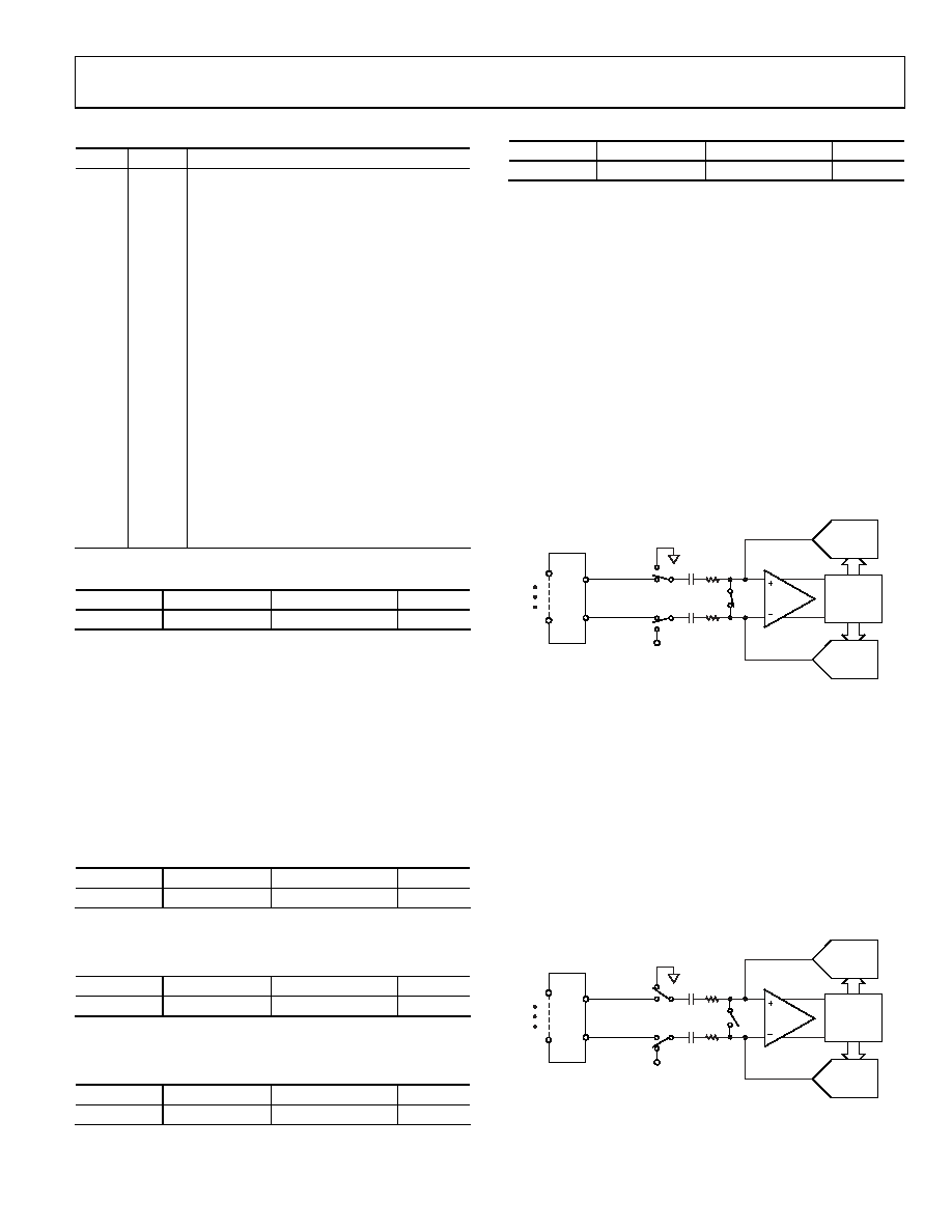
CONVERTER OPERATION
The ADC incorporates a successive approximation (SAR)
architecture involving a charge-sampled input stage. This
architecture can operate in three different modes: differential,
pseudo differential, and single-ended.
Differential Mode
The ADuC7019/20/21/22/24/25/26/27/28 each contain a
successive approximation ADC based on two capacitive DACs.
in acquisition and conversion phase, respectively. The ADC is
comprised of control logic, a SAR, and two capacitive DACs. In
Figure 43 (the acquisition phase), SW3 is closed and SW1 and
SW2 are in Position A. The comparator is held in a balanced
condition, and the sampling capacitor arrays acquire the
differential signal on the input.
0495
5-
0
17
CAPACITIVE
DAC
CAPACITIVE
DAC
CONTROL
LOGIC
COMPARATOR
SW3
SW1
A
B
SW2
CS
VREF
AIN0
AIN11
MUX
CHANNEL+
CHANNEL–
Figure 43. ADC Acquisition Phase
When the ADC starts a conversion, as shown in Figure 44, SW3
opens, and then SW1 and SW2 move to Position B. This causes
the comparator to become unbalanced. Both inputs are discon-
nected once the conversion begins. The control logic and the
charge redistribution DACs are used to add and subtract fixed
amounts of charge from the sampling capacitor arrays to bring
the comparator back into a balanced condition. When the
comparator is rebalanced, the conversion is complete. The
control logic generates the ADC’s output code. The output
impedances of the sources driving the VIN+ and VIN– pins must
be matched; otherwise, the two inputs have different settling
times, resulting in errors.
0495
5-
0
18
CAPACITIVE
DAC
CAPACITIVE
DAC
CONTROL
LOGIC
COMPARATOR
SW3
SW1
A
B
SW2
CS
VREF
AIN0
AIN11
MUX
CHANNEL+
CHANNEL–
Figure 44. ADC Conversion Phase
相关PDF资料 |
PDF描述 |
|---|---|
| ADUC7023BCPZ62I-R7 | IC MCU 12BIT 62KB FLASH 32LFCSP |
| ADUC7024BCPZ62 | IC MCU FLSH 62K ANLG I/O 64LFCSP |
| ADUC7032BSTZ-88 | IC MCU 96K FLASH DUAL 48LQFP |
| ADUC7032BSTZ-8V-RL | IC BATTERY SENSOR PREC 48-LQFP |
| ADUC7034BCPZ | IC MCU FLASH 32K ANLG IO 48LFCSP |
相关代理商/技术参数 |
参数描述 |
|---|---|
| ADUC7022 | 制造商:AD 制造商全称:Analog Devices 功能描述:Precision Analog Microcontroller 12-bit Analog I/O, ARM7TDMI MCU |
| ADUC7022ACP32 | 制造商:Analog Devices 功能描述:FLASH ARM7+10-CH,12-B ADC IC - Trays |
| ADUC7022ACPZ32 | 制造商:Analog Devices 功能描述:MCU 32BIT RISC 32KB FLASH 3.3V 40LFCSP EP - Trays |
| ADUC7022BCP32 | 制造商:Analog Devices 功能描述:FLASH ARM7+10-CH,12-B ADC IC - Trays |
| ADUC7022BCP62 | 制造商:Analog Devices 功能描述:FLASH ARM7+10-CH,12-B ADC IC - Trays |
发布紧急采购,3分钟左右您将得到回复。