- 您现在的位置:买卖IC网 > PDF目录1900 > ADUC7021BCPZ62-RL7 (Analog Devices Inc)IC MCU 12BIT 1MSPS UART 40-LFCSP PDF资料下载
参数资料
| 型号: | ADUC7021BCPZ62-RL7 |
| 厂商: | Analog Devices Inc |
| 文件页数: | 44/92页 |
| 文件大小: | 0K |
| 描述: | IC MCU 12BIT 1MSPS UART 40-LFCSP |
| 标准包装: | 750 |
| 系列: | MicroConverter® ADuC7xxx |
| 核心处理器: | ARM7 |
| 芯体尺寸: | 16/32-位 |
| 速度: | 44MHz |
| 连通性: | EBI/EMI,I²C,SPI,UART/USART |
| 外围设备: | PLA,PWM,PSM,温度传感器,WDT |
| 输入/输出数: | 13 |
| 程序存储器容量: | 64KB(32K x 16) |
| 程序存储器类型: | 闪存 |
| RAM 容量: | 2K x 32 |
| 电压 - 电源 (Vcc/Vdd): | 2.7 V ~ 3.6 V |
| 数据转换器: | A/D 8x12b,D/A 2x12b |
| 振荡器型: | 内部 |
| 工作温度: | -40°C ~ 125°C |
| 封装/外壳: | 40-VFQFN 裸露焊盘,CSP |
| 包装: | 带卷 (TR) |
第1页第2页第3页第4页第5页第6页第7页第8页第9页第10页第11页第12页第13页第14页第15页第16页第17页第18页第19页第20页第21页第22页第23页第24页第25页第26页第27页第28页第29页第30页第31页第32页第33页第34页第35页第36页第37页第38页第39页第40页第41页第42页第43页当前第44页第45页第46页第47页第48页第49页第50页第51页第52页第53页第54页第55页第56页第57页第58页第59页第60页第61页第62页第63页第64页第65页第66页第67页第68页第69页第70页第71页第72页第73页第74页第75页第76页第77页第78页第79页第80页第81页第82页第83页第84页第85页第86页第87页第88页第89页第90页第91页第92页
ADuC7019/20/21/22/24/25/26/27/28
Rev. B | Page 49 of 92
OTHER ANALOG PERIPHERALS
DAC
The ADuC7019/20/21/22/24/25/26/27/28 incorporate two,
three, or four, 12-bit voltage output DACs on-chip, depending on
the model. Each DAC has a rail-to-rail voltage output buffer
capable of driving 5 kΩ/100 pF.
Each DAC has three selectable ranges: 0 V to VREF (internal
band gap 2.5 V reference), 0 V to DACREF, and 0 V to AVDD.
DACREF is equivalent to an external reference for the DAC.
The signal range is 0 V to AVDD.
MMRs Interface
Each DAC is independently configurable through a control
register and a data register. These two registers are identical for
the four DACs. Only DAC0CON (see Table 27) and DAC0DAT
(see Table 28) are described in detail in this section.
DACxCON Registers
Name
Address
Default Value
Access
DAC0CON
0xFFFF0600
0x00
R/W
DAC1CON
0xFFFF0608
0x00
R/W
DAC2CON
0xFFFF0610
0x00
R/W
DAC3CON
0xFFFF0618
0x00
R/W
Table 27. DAC0CON MMR Bit Designations
Bit
Value
Name
Description
7:6
Reserved.
5
DACCLK
DAC Update Rate. Set by user to
update the DAC using Timer1.
Cleared by user to update the DAC
using HCLK (core clock).
4
DACCLR
DAC Clear Bit. Set by user to enable
normal DAC operation. Cleared by
user to reset data register of the DAC
to 0.
3
Reserved. This bit should be left at 0.
2
Reserved. This bit should be left at 0.
1:0
DAC Range Bits.
00
Power-Down Mode. The DAC output
is in tristate.
01
0 V to DACREF Range.
10
0 V to VREF (2.5 V) Range.
11
0 V to AVDD Range.
DACxDAT Registers
Name
Address
Default Value
Access
DAC0DAT
0xFFFF0604
0x00000000
R/W
DAC1DAT
0xFFFF060C
0x00000000
R/W
DAC2DAT
0xFFFF0614
0x00000000
R/W
DAC3DAT
0xFFFF061C
0x00000000
R/W
Table 28. DAC0DAT MMR Bit Designations
Bit
Description
31:28
Reserved.
27:16
12-Bit Data for DAC0.
15:0
Reserved.
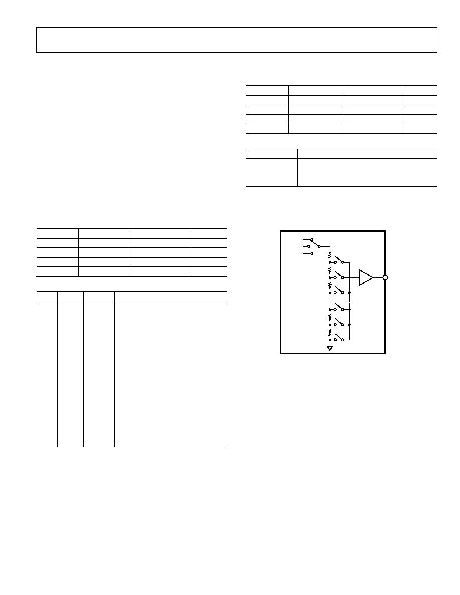
Using the DACs
The on-chip DAC architecture consists of a resistor string DAC
followed by an output buffer amplifier. The functional equivalent
is shown in Figure 52.
04
95
5-
02
3
R
DAC0
VREF
AVDD
DACREF
Figure 52. DAC Structure
As illustrated in Figure 52, the reference source for each DAC is
user-selectable in software. It can be either AVDD, VREF, or DACREF.
In 0-to-AVDD mode, the DAC output transfer function spans
from 0 V to the voltage at the AVDD pin. In 0-to-DACREF mode,
the DAC output transfer function spans from 0 V to the voltage at
the DACREF pin. In 0-to-VREF mode, the DAC output transfer
function spans from 0 V to the internal 2.5 V reference, VREF.
The DAC output buffer amplifier features a true, rail-to-rail
output stage implementation. This means that when unloaded,
each output is capable of swinging to within less than 5 mV of
both AVDD and ground. Moreover, the DAC’s linearity specification
(when driving a 5 kΩ resistive load to ground) is guaranteed
through the full transfer function except codes 0 to 100, and, in
0-to-AVDD mode only, codes 3995 to 4095.
相关PDF资料 |
PDF描述 |
|---|---|
| ADUC7023BCPZ62I-R7 | IC MCU 12BIT 62KB FLASH 32LFCSP |
| ADUC7024BCPZ62 | IC MCU FLSH 62K ANLG I/O 64LFCSP |
| ADUC7032BSTZ-88 | IC MCU 96K FLASH DUAL 48LQFP |
| ADUC7032BSTZ-8V-RL | IC BATTERY SENSOR PREC 48-LQFP |
| ADUC7034BCPZ | IC MCU FLASH 32K ANLG IO 48LFCSP |
相关代理商/技术参数 |
参数描述 |
|---|---|
| ADUC7022 | 制造商:AD 制造商全称:Analog Devices 功能描述:Precision Analog Microcontroller 12-bit Analog I/O, ARM7TDMI MCU |
| ADUC7022ACP32 | 制造商:Analog Devices 功能描述:FLASH ARM7+10-CH,12-B ADC IC - Trays |
| ADUC7022ACPZ32 | 制造商:Analog Devices 功能描述:MCU 32BIT RISC 32KB FLASH 3.3V 40LFCSP EP - Trays |
| ADUC7022BCP32 | 制造商:Analog Devices 功能描述:FLASH ARM7+10-CH,12-B ADC IC - Trays |
| ADUC7022BCP62 | 制造商:Analog Devices 功能描述:FLASH ARM7+10-CH,12-B ADC IC - Trays |
发布紧急采购,3分钟左右您将得到回复。