- 您现在的位置:买卖IC网 > PDF目录1900 > ADUC7021BCPZ62-RL7 (Analog Devices Inc)IC MCU 12BIT 1MSPS UART 40-LFCSP PDF资料下载
参数资料
| 型号: | ADUC7021BCPZ62-RL7 |
| 厂商: | Analog Devices Inc |
| 文件页数: | 58/92页 |
| 文件大小: | 0K |
| 描述: | IC MCU 12BIT 1MSPS UART 40-LFCSP |
| 标准包装: | 750 |
| 系列: | MicroConverter® ADuC7xxx |
| 核心处理器: | ARM7 |
| 芯体尺寸: | 16/32-位 |
| 速度: | 44MHz |
| 连通性: | EBI/EMI,I²C,SPI,UART/USART |
| 外围设备: | PLA,PWM,PSM,温度传感器,WDT |
| 输入/输出数: | 13 |
| 程序存储器容量: | 64KB(32K x 16) |
| 程序存储器类型: | 闪存 |
| RAM 容量: | 2K x 32 |
| 电压 - 电源 (Vcc/Vdd): | 2.7 V ~ 3.6 V |
| 数据转换器: | A/D 8x12b,D/A 2x12b |
| 振荡器型: | 内部 |
| 工作温度: | -40°C ~ 125°C |
| 封装/外壳: | 40-VFQFN 裸露焊盘,CSP |
| 包装: | 带卷 (TR) |
第1页第2页第3页第4页第5页第6页第7页第8页第9页第10页第11页第12页第13页第14页第15页第16页第17页第18页第19页第20页第21页第22页第23页第24页第25页第26页第27页第28页第29页第30页第31页第32页第33页第34页第35页第36页第37页第38页第39页第40页第41页第42页第43页第44页第45页第46页第47页第48页第49页第50页第51页第52页第53页第54页第55页第56页第57页当前第58页第59页第60页第61页第62页第63页第64页第65页第66页第67页第68页第69页第70页第71页第72页第73页第74页第75页第76页第77页第78页第79页第80页第81页第82页第83页第84页第85页第86页第87页第88页第89页第90页第91页第92页
ADuC7019/20/21/22/24/25/26/27/28
Rev. B | Page 61 of 92
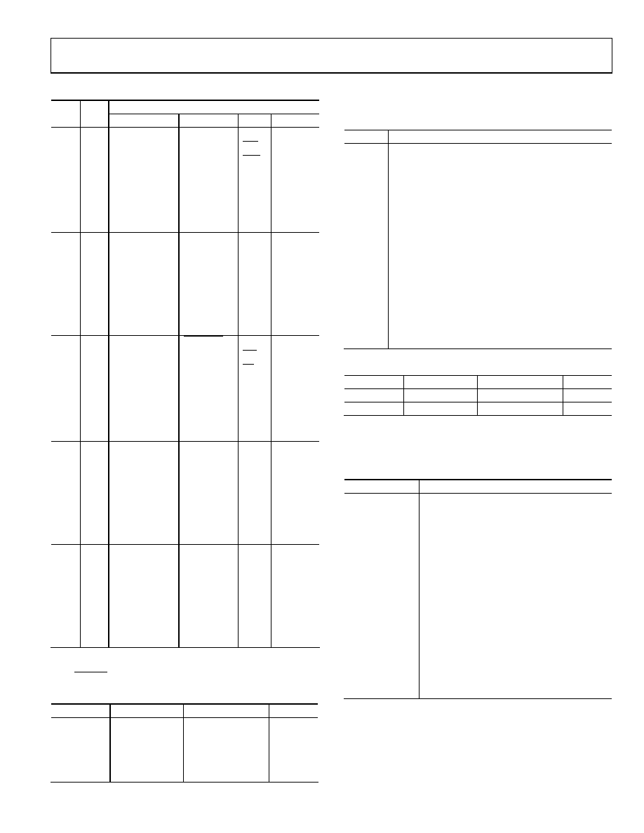
Table 40. GPIO Pin Function Descriptions
Configuration
Port
Pin
00
01
10
11
0
P0.0
GPIO
CMP
MS0
PLAI[7]
P0.1
GPIO
PWM2H
BLE
P0.2
GPIO
PWM2L
BHE
P0.3
GPIO
TRST
A16
ADCBUSY
P0.4
GPIO/IRQ0
PWMTRIP
MS1
PLAO[1]
P0.5
GPIO/IRQ1
ADCBUSY
MS2
PLAO[2]
P0.6
GPIO/T1
MRST
PLAO[3]
P0.7
GPIO
ECLK/XCLK1
SIN
PLAO[4]
1
P1.0
GPIO/T1
SIN
SCL0
PLAI[0]
P1.1
GPIO
SOUT
SDA0
PLAI[1]
P1.2
GPIO
RTS
SCL1
PLAI[2]
P1.3
GPIO
CTS
SDA1
PLAI[3]
P1.4
GPIO/IRQ2
RI
CLK
PLAI[4]
P1.5
GPIO/IRQ3
DCD
MISO
PLAI[5]
P1.6
GPIO
DSR
MOSI
PLAI[6]
P1.7
GPIO
DTR
CSL
PLAO[0]
2
P2.0
GPIO
CONVSTART2
SOUT
PLAO[5]
P2.1
GPIO
PWM0H
WS
PLAO[6]
P2.2
GPIO
PWM0L
RS
PLAO[7]
P2.3
GPIO
AE
P2.4
GPIO
PWM0H
MS0
P2.5
GPIO
PWM0L
MS1
P2.6
GPIO
PWM1H
MS2
P2.7
GPIO
PWM1L
MS3
3
P3.0
GPIO
PWM0H
AD0
PLAI[8]
P3.1
GPIO
PWM0L
AD1
PLAI[9]
P3.2
GPIO
PWM1H
AD2
PLAI[10]
P3.3
GPIO
PWM1L
AD3
PLAI[11]
P3.4
GPIO
PWM2H
AD4
PLAI[12]
P3.5
GPIO
PWM2L
AD5
PLAI[13]
P3.6
GPIO
PWMTRIP
AD6
PLAI[14]
P3.7
GPIO
PWMSYNC
AD7
PLAI[15]
4
P4.0
GPIO
AD8
PLAO[8]
P4.1
GPIO
AD9
PLAO[9]
P4.2
GPIO
AD10
PLAO[10]
P4.3
GPIO
AD11
PLAO[11]
P4.4
GPIO
AD12
PLAO[12]
P4.5
GPIO
AD13
PLAO[13]
P4.6
GPIO
AD14
PLAO[14]
P4.7
GPIO
AD15
PLAO[15]
1 When configured in Mode 1, P0.7 is ECLK by default, or core clock output.
To configure it as a clock input, the MDCLK bits in PLLCON must be set to 11.
2 The CONVSTART signal is active in all modes of P2.0.
GPxCON Registers
Name
Address
Default Value
Access
GP0CON
0xFFFFF400
0x00000000
R/W
GP1CON
0xFFFFF404
0x00000000
R/W
GP2CON
0xFFFFF408
0x00000000
R/W
GP3CON
0xFFFFF40C
0x00000000
R/W
GP4CON
0xFFFFF410
0x00000000
R/W
GPxCON are the Port x control registers, which select the
function of each pin of Port x as described in Table 41.
Table 41. GPxCON MMR Bit Descriptions
Bit
Description
31:30
Reserved.
29:28
Select Function of Px.7 Pin.
27:26
Reserved.
25:24
Select Function of Px.6 Pin.
23:22
Reserved.
21:20
Select Function of Px.5 Pin.
19:18
Reserved.
17:16
Select Function of Px.4 Pin.
15:14
Reserved.
13:12
Select Function of Px.3 Pin.
11:10
Reserved.
9:8
Select Function of Px.2 Pin.
7:6
Reserved.
5:4
Select Function of Px.1 Pin.
3:2
Reserved.
1:0
Select Function of Px.0 Pin.
GPxPAR Registers
Name
Address
Default Value
Access
GP0PAR
0xFFFFF42C
0x20000000
R/W
GP1PAR
0xFFFFF43C
0x00000000
R/W
GPxPAR program the parameters for Port 0 and Port 1. Note that
the GPxDAT MMR must always be written after changing the
GPxPAR MMR.
Table 42. GPxPAR MMR Bit Descriptions
Bit
Description
31:29
Reserved.
28
Pull-Up Disable Px.7.
27:25
Reserved.
24
Pull-Up Disable Px.6.
23:21
Reserved.
20
Pull-Up Disable Px.5.
19:17
Reserved.
16
Pull-Up Disable Px.4.
15:13
Reserved.
12
Pull-Up Disable Px.3.
11:9
Reserved.
8
Pull-Up Disable Px.2.
7:5
Reserved.
4
Pull-Up Disable Px.1.
3:1
Reserved.
0
Pull-Up Disable Px.0.
相关PDF资料 |
PDF描述 |
|---|---|
| ADUC7023BCPZ62I-R7 | IC MCU 12BIT 62KB FLASH 32LFCSP |
| ADUC7024BCPZ62 | IC MCU FLSH 62K ANLG I/O 64LFCSP |
| ADUC7032BSTZ-88 | IC MCU 96K FLASH DUAL 48LQFP |
| ADUC7032BSTZ-8V-RL | IC BATTERY SENSOR PREC 48-LQFP |
| ADUC7034BCPZ | IC MCU FLASH 32K ANLG IO 48LFCSP |
相关代理商/技术参数 |
参数描述 |
|---|---|
| ADUC7022 | 制造商:AD 制造商全称:Analog Devices 功能描述:Precision Analog Microcontroller 12-bit Analog I/O, ARM7TDMI MCU |
| ADUC7022ACP32 | 制造商:Analog Devices 功能描述:FLASH ARM7+10-CH,12-B ADC IC - Trays |
| ADUC7022ACPZ32 | 制造商:Analog Devices 功能描述:MCU 32BIT RISC 32KB FLASH 3.3V 40LFCSP EP - Trays |
| ADUC7022BCP32 | 制造商:Analog Devices 功能描述:FLASH ARM7+10-CH,12-B ADC IC - Trays |
| ADUC7022BCP62 | 制造商:Analog Devices 功能描述:FLASH ARM7+10-CH,12-B ADC IC - Trays |
发布紧急采购,3分钟左右您将得到回复。