- 您现在的位置:买卖IC网 > PDF目录1900 > ADUC7021BCPZ62-RL7 (Analog Devices Inc)IC MCU 12BIT 1MSPS UART 40-LFCSP PDF资料下载
参数资料
| 型号: | ADUC7021BCPZ62-RL7 |
| 厂商: | Analog Devices Inc |
| 文件页数: | 63/92页 |
| 文件大小: | 0K |
| 描述: | IC MCU 12BIT 1MSPS UART 40-LFCSP |
| 标准包装: | 750 |
| 系列: | MicroConverter® ADuC7xxx |
| 核心处理器: | ARM7 |
| 芯体尺寸: | 16/32-位 |
| 速度: | 44MHz |
| 连通性: | EBI/EMI,I²C,SPI,UART/USART |
| 外围设备: | PLA,PWM,PSM,温度传感器,WDT |
| 输入/输出数: | 13 |
| 程序存储器容量: | 64KB(32K x 16) |
| 程序存储器类型: | 闪存 |
| RAM 容量: | 2K x 32 |
| 电压 - 电源 (Vcc/Vdd): | 2.7 V ~ 3.6 V |
| 数据转换器: | A/D 8x12b,D/A 2x12b |
| 振荡器型: | 内部 |
| 工作温度: | -40°C ~ 125°C |
| 封装/外壳: | 40-VFQFN 裸露焊盘,CSP |
| 包装: | 带卷 (TR) |
第1页第2页第3页第4页第5页第6页第7页第8页第9页第10页第11页第12页第13页第14页第15页第16页第17页第18页第19页第20页第21页第22页第23页第24页第25页第26页第27页第28页第29页第30页第31页第32页第33页第34页第35页第36页第37页第38页第39页第40页第41页第42页第43页第44页第45页第46页第47页第48页第49页第50页第51页第52页第53页第54页第55页第56页第57页第58页第59页第60页第61页第62页当前第63页第64页第65页第66页第67页第68页第69页第70页第71页第72页第73页第74页第75页第76页第77页第78页第79页第80页第81页第82页第83页第84页第85页第86页第87页第88页第89页第90页第91页第92页
ADuC7019/20/21/22/24/25/26/27/28
Rev. B | Page 66 of 92
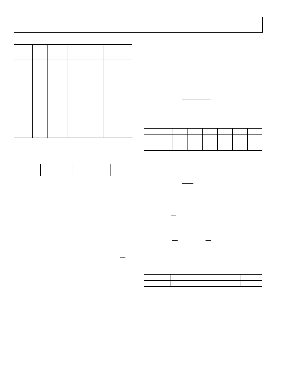
Table 57. COMIID1 MMR Bit Descriptions
Bit 3:1
Status
Bits
Bit 0
NINT
Priority
Definition
Clearing
Operation
000
1
–
No Interrupt.
–
110
0
2
Matching
Network Address.
Read COMRX.
101
0
3
Address
Transmitted,
Buffer Empty.
Write data to
COMTX or
read COMIID0.
011
0
1
Receive Line
Status Interrupt.
Read
COMSTA0.
010
0
2
Receive Buffer Full
Interrupt.
Read COMRX.
001
0
3
Transmit Buffer
Empty Interrupt.
Write data to
COMTX or
read COMIID0.
000
0
4
Modem Status
Interrupt.
Read
COMSTA1.
Note that to receive a network address interrupt, the slave must
ensure that Bit 0 of COMIEN0 (enable receive buffer full interrupt)
is set to 1.
COMADR Register
Name
Address
Default Value
Access
COMADR
0xFFFF0728
0xAA
R/W
COMADR is an 8-bit, read/write network address register that
holds the address checked for by the network addressable
UART. Upon receiving this address, the device interrupts the
processor and/or sets the appropriate status bit in COMIID1.
SERIAL PERIPHERAL INTERFACE
The ADuC7019/20/21/22/24/25/26/27/28 integrate a complete
hardware serial peripheral interface (SPI) on-chip. SPI is an indus-
try standard, synchronous serial interface that allows eight bits
of data to be synchronously transmitted and simultaneously
received, that is, full duplex up to a maximum bit rate of 3.48 Mb
as shown in Table 58. The SPI interface is not operational with core
clock divider (CD) bits. POWCON[2:0] = 6 or 7 in master mode.
The SPI port can be configured for master or slave operation
and typically consists of four pins: MISO, MOSI, SCL, and CS.
MISO (Master In, Slave Out) Pin
The MISO pin is configured as an input line in master mode
and an output line in slave mode. The MISO line on the master
(data in) should be connected to the MISO line in the slave
device (data out). The data is transferred as byte wide (8-bit)
serial data, MSB first.
MOSI (Master Out, Slave In) Pin
The MOSI pin is configured as an output line in master mode
and an input line in slave mode. The MOSI line on the master
(data out) should be connected to the MOSI line in the slave
device (data in). The data is transferred as byte wide (8-bit)
serial data, MSB first.
SCL (Serial Clock I/O) Pin
The master serial clock (SCL) is used to synchronize the data
being transmitted and received through the MOSI SCL period.
Therefore, a byte is transmitted/received after eight SCL periods.
The SCL pin is configured as an output in master mode and as
an input in slave mode.
In master mode, polarity and phase of the clock are controlled
by the SPICON register, and the bit rate is defined in the
SPIDIV register as follows:
)
1
(
2
SPIDIV
f
UCLK
CLOCK
SERIAL
+
×
=
The maximum speed of the SPI clock is dependent on the clock
divider bits and is summarized in Table 58.
Table 58. SPI Speed vs. Clock Divider Bits in Master Mode
CD Bits
0
1
2
3
4
5
SPIDIV in hex
0x05
0x0B
0x17
0x2F
0x5F
0xBF
SPI speed
in MHz
3.482
1.741
0.870
0.435
0.218
0.109
In slave mode, the SPICON register must be configured with
the phase and polarity of the expected input clock. The slave
accepts data from an external master up to 10.4 Mb at CD = 0.
The formula to determine the maximum speed is as follows:
4
HCLK
CLOCK
SERIAL
f
=
In both master and slave modes, data is transmitted on one edge
of the SCL signal and sampled on the other. Therefore, it is
important that the polarity and phase are configured the same
for the master and slave devices.
Chip Select (CS Input) Pin
In SPI slave mode, a transfer is initiated by the assertion of CS,
which is an active low input signal. The SPI port then transmits
and receives 8-bit data until the transfer is concluded by
deassertion of CS. In slave mode, CS is always an input.
SPI Registers
The following MMR registers are used to control the SPI
interface: SPISTA, SPIRX, SPITX, SPIDIV, and SPICON.
SPISTA Register
Name
Address
Default Value
Access
SPISTA
0xFFFF0A00
0x00
R/W
SPISTA is an 8-bit read-only status register. Only Bit 1 or Bit 4
of this register generates an interrupt. Bit 6 of the SPICON
register determines which bit generates the interrupt.
相关PDF资料 |
PDF描述 |
|---|---|
| ADUC7023BCPZ62I-R7 | IC MCU 12BIT 62KB FLASH 32LFCSP |
| ADUC7024BCPZ62 | IC MCU FLSH 62K ANLG I/O 64LFCSP |
| ADUC7032BSTZ-88 | IC MCU 96K FLASH DUAL 48LQFP |
| ADUC7032BSTZ-8V-RL | IC BATTERY SENSOR PREC 48-LQFP |
| ADUC7034BCPZ | IC MCU FLASH 32K ANLG IO 48LFCSP |
相关代理商/技术参数 |
参数描述 |
|---|---|
| ADUC7022 | 制造商:AD 制造商全称:Analog Devices 功能描述:Precision Analog Microcontroller 12-bit Analog I/O, ARM7TDMI MCU |
| ADUC7022ACP32 | 制造商:Analog Devices 功能描述:FLASH ARM7+10-CH,12-B ADC IC - Trays |
| ADUC7022ACPZ32 | 制造商:Analog Devices 功能描述:MCU 32BIT RISC 32KB FLASH 3.3V 40LFCSP EP - Trays |
| ADUC7022BCP32 | 制造商:Analog Devices 功能描述:FLASH ARM7+10-CH,12-B ADC IC - Trays |
| ADUC7022BCP62 | 制造商:Analog Devices 功能描述:FLASH ARM7+10-CH,12-B ADC IC - Trays |
发布紧急采购,3分钟左右您将得到回复。