- 您现在的位置:买卖IC网 > PDF目录1900 > ADUC7021BCPZ62-RL7 (Analog Devices Inc)IC MCU 12BIT 1MSPS UART 40-LFCSP PDF资料下载
参数资料
| 型号: | ADUC7021BCPZ62-RL7 |
| 厂商: | Analog Devices Inc |
| 文件页数: | 37/92页 |
| 文件大小: | 0K |
| 描述: | IC MCU 12BIT 1MSPS UART 40-LFCSP |
| 标准包装: | 750 |
| 系列: | MicroConverter® ADuC7xxx |
| 核心处理器: | ARM7 |
| 芯体尺寸: | 16/32-位 |
| 速度: | 44MHz |
| 连通性: | EBI/EMI,I²C,SPI,UART/USART |
| 外围设备: | PLA,PWM,PSM,温度传感器,WDT |
| 输入/输出数: | 13 |
| 程序存储器容量: | 64KB(32K x 16) |
| 程序存储器类型: | 闪存 |
| RAM 容量: | 2K x 32 |
| 电压 - 电源 (Vcc/Vdd): | 2.7 V ~ 3.6 V |
| 数据转换器: | A/D 8x12b,D/A 2x12b |
| 振荡器型: | 内部 |
| 工作温度: | -40°C ~ 125°C |
| 封装/外壳: | 40-VFQFN 裸露焊盘,CSP |
| 包装: | 带卷 (TR) |
第1页第2页第3页第4页第5页第6页第7页第8页第9页第10页第11页第12页第13页第14页第15页第16页第17页第18页第19页第20页第21页第22页第23页第24页第25页第26页第27页第28页第29页第30页第31页第32页第33页第34页第35页第36页当前第37页第38页第39页第40页第41页第42页第43页第44页第45页第46页第47页第48页第49页第50页第51页第52页第53页第54页第55页第56页第57页第58页第59页第60页第61页第62页第63页第64页第65页第66页第67页第68页第69页第70页第71页第72页第73页第74页第75页第76页第77页第78页第79页第80页第81页第82页第83页第84页第85页第86页第87页第88页第89页第90页第91页第92页
ADuC7019/20/21/22/24/25/26/27/28
Rev. B | Page 42 of 92
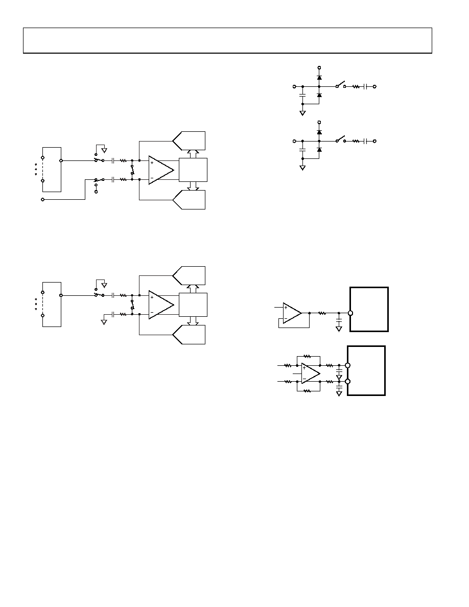
Pseudo Differential Mode
In pseudo differential mode, Channel is linked to the VIN pin
of the ADuC7019/20/21/22/24/25/26/27/28. SW2 switches
between A (Channel) and B (VREF). VIN pin must be
connected to ground or a low voltage. The input signal on VIN+
can then vary from VIN to VREF + VIN. Note that VIN must be
chosen so that VREF + VIN do not exceed AVDD.
0495
5-
0
19
CAPACITIVE
DAC
CAPACITIVE
DAC
CONTROL
LOGIC
COMPARATOR
SW3
SW1
A
B
SW2
CS
VREF
AIN0
AIN11
VIN–
MUX
CHANNEL+
CHANNEL–
Figure 45. ADC in Pseudo Differential Mode
Single-Ended Mode
In single-ended mode, SW2 is always connected internally to
ground. The VIN pin can be floating. The input signal range on
VIN+ is 0 V to VREF.
0495
5-
0
20
CAPACITIVE
DAC
CAPACITIVE
DAC
CONTROL
LOGIC
COMPARATOR
SW3
SW1
A
B
CS
AIN0
AIN11
MUX
CHANNEL+
CHANNEL–
Figure 46. ADC in Single-Ended Mode
Analog Input Structure
Figure 47 shows the equivalent circuit of the analog input structure
of the ADC. The four diodes provide ESD protection for the analog
inputs. Care must be taken to ensure that the analog input
signals never exceed the supply rails by more than 300 mV; this
would cause these diodes to become forward-biased and start
conducting into the substrate. These diodes can conduct up to
10 mA without causing irreversible damage to the part.
The C1 capacitors in Figure 47 are typically 4 pF and can be
primarily attributed to pin capacitance. The resistors are
lumped components made up of the on resistance of the
switches. The value of these resistors is typically about 100 Ω.
The C2 capacitors are the ADC’s sampling capacitors and
typically have a capacitance of 16 pF.
AVDD
C1
D
R1 C2
AVDD
C1
D
R1 C2
04
95
5-
0
21
Figure 47. Equivalent Analog Input Circuit Conversion Phase: Switches Open,
Track Phase: Switches Closed
For ac applications, removing high frequency components from
the analog input signal is recommended by using an RC low-
pass filter on the relevant analog input pins. In applications
where harmonic distortion and signal-to-noise ratio are critical,
the analog input should be driven from a low impedance
source. Large source impedances significantly affect the ac
performance of the ADC. This can necessitate the use of an
input buffer amplifier. The choice of the op amp is a function of
example of ADC front end.
0
495
5-
0
61
ADuC7019/
ADuC702x
ADC0
10
0.01F
Figure 48. Buffering Single-Ended/Pseudo Differential Input
04
95
5-
0
62
ADuC7019/
ADuC702x
ADC0
VREF
ADC1
Figure 49. Buffering Differential Inputs
When no amplifier is used to drive the analog input, the source
impedance should be limited to values lower than 1 kΩ. The
maximum source impedance depends on the amount of total
harmonic distortion (THD) that can be tolerated. The THD
increases as the source impedance increases and the performance
degrades.
DRIVING THE ANALOG INPUTS
Internal or external references can be used for the ADC. In
differential mode of operation, there are restrictions on the
common-mode input signal (VCM), which is dependent upon
the reference value and supply voltage used to ensure that the
signal remains within the supply rails. Table 18 gives some
calculated VCM minimum and VCM maximum values.
相关PDF资料 |
PDF描述 |
|---|---|
| ADUC7023BCPZ62I-R7 | IC MCU 12BIT 62KB FLASH 32LFCSP |
| ADUC7024BCPZ62 | IC MCU FLSH 62K ANLG I/O 64LFCSP |
| ADUC7032BSTZ-88 | IC MCU 96K FLASH DUAL 48LQFP |
| ADUC7032BSTZ-8V-RL | IC BATTERY SENSOR PREC 48-LQFP |
| ADUC7034BCPZ | IC MCU FLASH 32K ANLG IO 48LFCSP |
相关代理商/技术参数 |
参数描述 |
|---|---|
| ADUC7022 | 制造商:AD 制造商全称:Analog Devices 功能描述:Precision Analog Microcontroller 12-bit Analog I/O, ARM7TDMI MCU |
| ADUC7022ACP32 | 制造商:Analog Devices 功能描述:FLASH ARM7+10-CH,12-B ADC IC - Trays |
| ADUC7022ACPZ32 | 制造商:Analog Devices 功能描述:MCU 32BIT RISC 32KB FLASH 3.3V 40LFCSP EP - Trays |
| ADUC7022BCP32 | 制造商:Analog Devices 功能描述:FLASH ARM7+10-CH,12-B ADC IC - Trays |
| ADUC7022BCP62 | 制造商:Analog Devices 功能描述:FLASH ARM7+10-CH,12-B ADC IC - Trays |
发布紧急采购,3分钟左右您将得到回复。