- 您现在的位置:买卖IC网 > PDF目录1900 > ADUC7021BCPZ62-RL7 (Analog Devices Inc)IC MCU 12BIT 1MSPS UART 40-LFCSP PDF资料下载
参数资料
| 型号: | ADUC7021BCPZ62-RL7 |
| 厂商: | Analog Devices Inc |
| 文件页数: | 42/92页 |
| 文件大小: | 0K |
| 描述: | IC MCU 12BIT 1MSPS UART 40-LFCSP |
| 标准包装: | 750 |
| 系列: | MicroConverter® ADuC7xxx |
| 核心处理器: | ARM7 |
| 芯体尺寸: | 16/32-位 |
| 速度: | 44MHz |
| 连通性: | EBI/EMI,I²C,SPI,UART/USART |
| 外围设备: | PLA,PWM,PSM,温度传感器,WDT |
| 输入/输出数: | 13 |
| 程序存储器容量: | 64KB(32K x 16) |
| 程序存储器类型: | 闪存 |
| RAM 容量: | 2K x 32 |
| 电压 - 电源 (Vcc/Vdd): | 2.7 V ~ 3.6 V |
| 数据转换器: | A/D 8x12b,D/A 2x12b |
| 振荡器型: | 内部 |
| 工作温度: | -40°C ~ 125°C |
| 封装/外壳: | 40-VFQFN 裸露焊盘,CSP |
| 包装: | 带卷 (TR) |
第1页第2页第3页第4页第5页第6页第7页第8页第9页第10页第11页第12页第13页第14页第15页第16页第17页第18页第19页第20页第21页第22页第23页第24页第25页第26页第27页第28页第29页第30页第31页第32页第33页第34页第35页第36页第37页第38页第39页第40页第41页当前第42页第43页第44页第45页第46页第47页第48页第49页第50页第51页第52页第53页第54页第55页第56页第57页第58页第59页第60页第61页第62页第63页第64页第65页第66页第67页第68页第69页第70页第71页第72页第73页第74页第75页第76页第77页第78页第79页第80页第81页第82页第83页第84页第85页第86页第87页第88页第89页第90页第91页第92页
ADuC7019/20/21/22/24/25/26/27/28
Rev. B | Page 47 of 92
EXECUTION TIME FROM SRAM AND FLASH/EE
Execution from SRAM
Fetching instructions from SRAM takes one clock cycle as the
access time of the SRAM is 2 ns and a clock cycle is 22 ns
minimum. However, if the instruction involves reading or
writing data to memory, one extra cycle must be added if the
data is in SRAM (or three cycles if the data is in Flash/EE); one
cycle to execute the instruction, and two cycles to get the 32-bit
data from Flash/EE. A control flow instruction (a branch
instruction, for example) takes one cycle to fetch but also takes
two cycles to fill the pipeline with the new instructions.
Execution from Flash/EE
Because the Flash/EE width is 16 bits and access time for 16-bit
words is 22 ns, execution from Flash/EE cannot be done in
one cycle (as can be done from SRAM when CD Bit = 0). Also,
some dead times are needed before accessing data for any value
of CD bits.
In ARM mode, where instructions are 32 bits, two cycles are
needed to fetch any instruction when CD = 0. In thumb mode,
where instructions are 16 bits, one cycle is needed to fetch any
instruction.
Timing is identical in both modes when executing instructions
that involve using the Flash/EE for data memory. If the
instruction to be executed is a control flow instruction, an extra
cycle is needed to decode the new address of the program
counter, and then four cycles are needed to fill the pipeline. A
data-processing instruction involving only the core register
does not require any extra clock cycles. However, if it involves
data in Flash/EE, an extra clock cycle is needed to decode the
address of the data, and two cycles are needed to get the 32-bit
data from Flash/EE. An extra cycle must also be added before
fetching another instruction. Data transfer instructions are
more complex and are summarized in Table 24.
Table 24. Execution Cycles in ARM/Thumb Mode
Instructions
Fetch
Cycles
Dead
Time
Data Access
Dead
Time
2/1
1
2
1
LDH
2/1
1
2/1
N2
2 × N2
2/1
1
2 × 20 ns
1
STRH
2/1
20 ns
1
STRM/POP
2/1
2 × N × 20 ns1
1 The SWAP instruction combines an LD and STR instruction with only one
fetch, giving a total of eight cycles + 40 ns.
2 N is the number of data to load or store in the multiple load/store instruction
(1 < N ≤ 16).
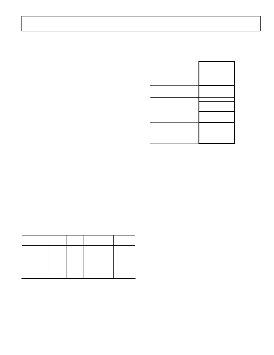
RESET AND REMAP
The ARM exception vectors are all situated at the bottom of the
memory array, from Address 0x00000000 to Address 0x00000020
as shown in Figure 51.
04
955
-02
2
KERNEL
INTERRUPT
SERVICE ROUTINES
INTERRUPT
SERVICE ROUTINES
ARM EXCEPTION
VECTOR ADDRESSES
0x00000020
0x00011FFF
0x0008FFFF
0xFFFFFFFF
FLASH/EE
SRAM
MIRROR SPACE
0x00000000 0x00000000
0x00010000
0x00080000
Figure 51. Remap for Exception Execution
By default, and after any reset, the Flash/EE is mirrored at the
bottom of the memory array. The remap function allows the
programmer to mirror the SRAM at the bottom of the memory
array, which facilitates execution of exception routines from
SRAM instead of from Flash/EE. This means exceptions are
executed twice as fast, being executed in 32-bit ARM mode with
32-bit wide SRAM instead of 16-bit wide Flash/EE memory.
Remap Operation
When a reset occurs on the ADuC7019/20/21/22/24/25/26/27/28,
execution automatically starts in factory-programmed, internal
configuration code. This kernel is hidden and cannot be accessed
by user code. If the part is in normal mode (BM pin is high), it
executes the power-on configuration routine of the kernel and
then jumps to the reset vector address, 0x00000000, to execute
the user’s reset exception routine.
Because the Flash/EE is mirrored at the bottom of the memory
array at reset, the reset interrupt routine must always be written
in Flash/EE.
The remap is done from Flash/EE by setting Bit 0 of the REMAP
register. Caution must be taken to execute this command from
Flash/EE, above Address 0x00080020, and not from the bottom
of the array, as this is replaced by the SRAM.
This operation is reversible. The Flash/EE can be remapped at
Address 0x00000000 by clearing Bit 0 of the REMAP MMR.
Caution must again be taken to execute the remap function
from outside the mirrored area. Any type of reset remaps the
Flash/EE memory at the bottom of the array.
相关PDF资料 |
PDF描述 |
|---|---|
| ADUC7023BCPZ62I-R7 | IC MCU 12BIT 62KB FLASH 32LFCSP |
| ADUC7024BCPZ62 | IC MCU FLSH 62K ANLG I/O 64LFCSP |
| ADUC7032BSTZ-88 | IC MCU 96K FLASH DUAL 48LQFP |
| ADUC7032BSTZ-8V-RL | IC BATTERY SENSOR PREC 48-LQFP |
| ADUC7034BCPZ | IC MCU FLASH 32K ANLG IO 48LFCSP |
相关代理商/技术参数 |
参数描述 |
|---|---|
| ADUC7022 | 制造商:AD 制造商全称:Analog Devices 功能描述:Precision Analog Microcontroller 12-bit Analog I/O, ARM7TDMI MCU |
| ADUC7022ACP32 | 制造商:Analog Devices 功能描述:FLASH ARM7+10-CH,12-B ADC IC - Trays |
| ADUC7022ACPZ32 | 制造商:Analog Devices 功能描述:MCU 32BIT RISC 32KB FLASH 3.3V 40LFCSP EP - Trays |
| ADUC7022BCP32 | 制造商:Analog Devices 功能描述:FLASH ARM7+10-CH,12-B ADC IC - Trays |
| ADUC7022BCP62 | 制造商:Analog Devices 功能描述:FLASH ARM7+10-CH,12-B ADC IC - Trays |
发布紧急采购,3分钟左右您将得到回复。