- 您现在的位置:买卖IC网 > PDF目录67672 > GT-48001A (Galileo Technology Services, LLC) Switched Ethernet Controller For 10BaseX(10BaseX交换式快速以太网控制器) PDF资料下载
参数资料
| 型号: | GT-48001A |
| 厂商: | Galileo Technology Services, LLC |
| 英文描述: | Switched Ethernet Controller For 10BaseX(10BaseX交换式快速以太网控制器) |
| 中文描述: | 交换式以太网控制器10BaseX(10BaseX交换式快速以太网控制器) |
| 文件页数: | 18/101页 |
| 文件大小: | 1235K |
| 代理商: | GT-48001A |
第1页第2页第3页第4页第5页第6页第7页第8页第9页第10页第11页第12页第13页第14页第15页第16页第17页当前第18页第19页第20页第21页第22页第23页第24页第25页第26页第27页第28页第29页第30页第31页第32页第33页第34页第35页第36页第37页第38页第39页第40页第41页第42页第43页第44页第45页第46页第47页第48页第49页第50页第51页第52页第53页第54页第55页第56页第57页第58页第59页第60页第61页第62页第63页第64页第65页第66页第67页第68页第69页第70页第71页第72页第73页第74页第75页第76页第77页第78页第79页第80页第81页第82页第83页第84页第85页第86页第87页第88页第89页第90页第91页第92页第93页第94页第95页第96页第97页第98页第99页第100页第101页
GT-48001A Switched Ethernet Controller
Revision 1.6
23
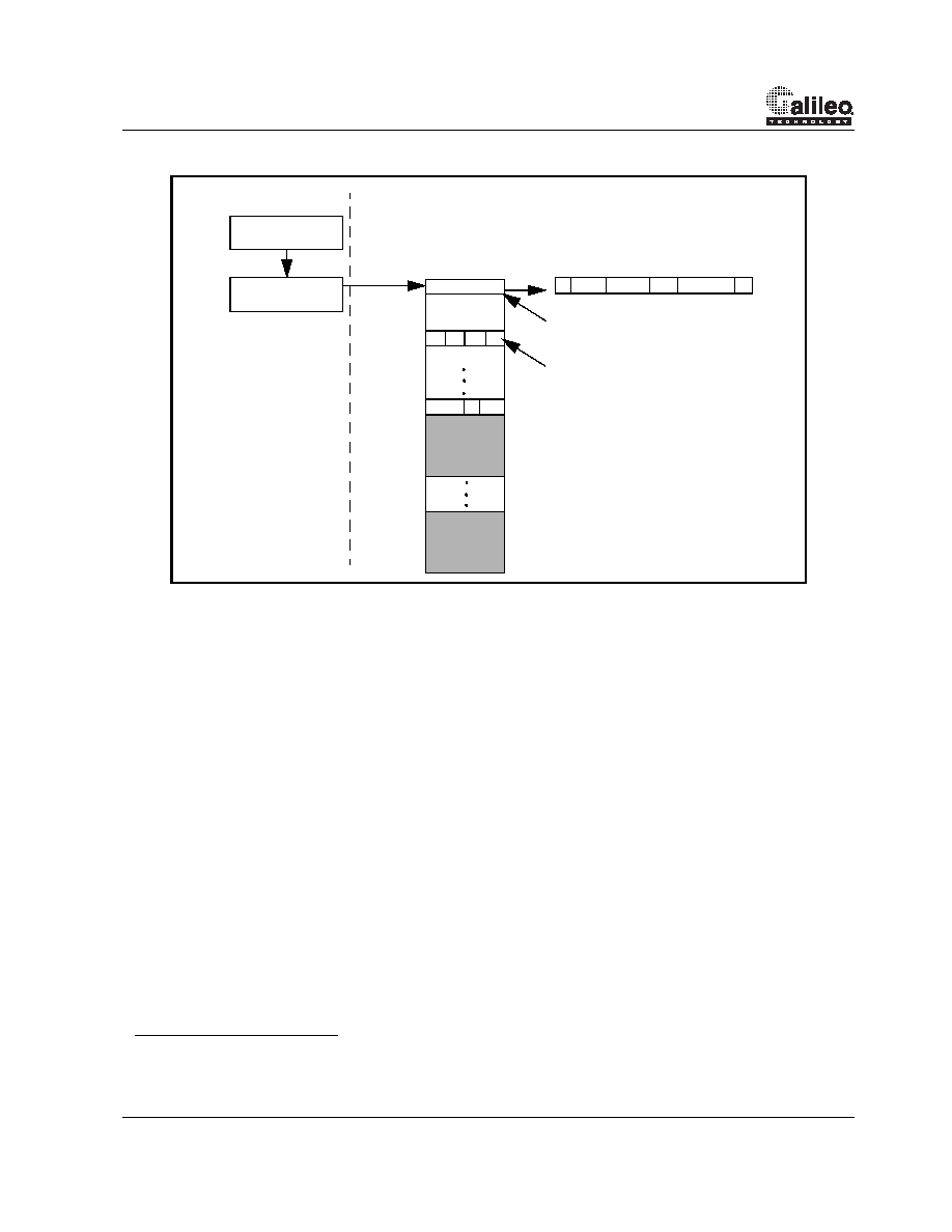
Figure 3: CPU Memory Data Structure
The data structure components are the following:
CPU Base Address Register (CBA)1 - A register that points to the beginning of a sixteen block area in CPU
memory.
CPU Base Address Shadow Register (CBAS) - A second register that holds a pointer to a second sixteen
block area in the CPU main memory. The value in the Shadow register propagates into the Base Address reg-
ister after sixteen packets are transferred to the main memory.
Buffer Area - The CPU buffer area consists of 16 blocks of 2Kbytes each. The first word (Word #0) of each
block contains the Sniffer Indication [31], EASE indication [23:15], Source Port Number [14:12], Byte Count
(bits [11:1]), and the Valid bit (bit 0). These bits are written as the END_OF_PACKET (Section 10.3.10) mes-
sage transferred from the source GT-48001A to the CPU at the end of a valid packet transfer. Words 1 to 7 are
left empty for user purposes.
The communication between the GT-48001A and the CPU follows this sequence:
1.
Upon initialization, CPU updates the CBA (1st write to 0x140034).
2.
Following the initial write to the CBA, the CPU updates the CBAS (2nd write to 0x140034).
3.
GT-48001A transfers 16 packets to the CPU main memory and asserts the Int* at the end of each packet transfer.
4.
The CPU must count sixteen interrupts and then update the Shadow register in the GT-48001A (write to
0x140034). Also, the BufWrap interrupt can be checked instead of counting sixteen interrupts. In other words, the
CPU must update 0x140034 ONCE after 16 packets have been transferred from the GT-48001A to the CPU. This
single word write after sixteen packets have been transferred to the CPU are to update the Shadow register only.
1. Assuming CBA and CBAS have already been written to, any writes to 0x140034 will update the CBAS register ONLY. In other words,
CBA can only be updated on the first write, and after 16 packets have been written to the CPU where the CBA will take the value of the
CBAS.
Block #1
Block #2
Block #16
0
1
2
3
n-1
n
31
0
Word#8,
BASE ADDRESS
REGISTER
Byte#32
GT-48001A
CPU Memory
BASE ADDRESS
SHADOW
S
31
EASE
23
15
SP
14 12
BC
V
11
1
0
Word#0,
Byte#0
相关PDF资料 |
PDF描述 |
|---|---|
| GT-48002A | Switched Fast Ethernet Controller for 100BaseX(100BaseX交换式快速以太网控制器) |
| GT-48004A | Four Port Switched Fast Ethernet Controller(四端口、交换式快速以太网控制器) |
| GT-48006A | Low Cost Two Port 10/100Mbps Ethernet Bridge/Switch Controller(低成本、双端口10/100Mbps以太网桥式/交换式控制器) |
| GT-48207 | Advanced Switched Ethernet Controllers for 10+10/100 BaseX(高级交换式 10+10/100 BaseX以太网控制器) |
| GT-48208 | Advanced Switched Ethernet Controllers for 10+10/100 BaseX(高级交换式 10+10/100 BaseX以太网控制器) |
相关代理商/技术参数 |
参数描述 |
|---|---|
| GT482 | 制造商:CORNELL DUBILIER ELECTRONICS 功能描述:Cap Ceramic 82pF 3000V SL 5% (12 X 6mm) Radial 9.5mm 85°C |
| GT48212-A6-PBB1C000 | 制造商:Marvell 功能描述: |
| GT48212-A6-PBB-C000 | 制造商:Marvell 功能描述:12 PORT E + 2 PORT FE SWITCH (MANAGED) - Trays |
| GT48300-A1-BBE1C083 | 制造商:Marvell 功能描述:Marvell GT48300-A1-BBE1C083 |
| GT48300-A1-BBE-C000 | 制造商:Marvell 功能描述:Marvell GT48300-A1-BBE-C000 |
发布紧急采购,3分钟左右您将得到回复。