- 您现在的位置:买卖IC网 > PDF目录224103 > K4T56163QI-ZLD50 16M X 16 SYNCHRONOUS DRAM, 0.5 ns, PBGA84 PDF资料下载
参数资料
| 型号: | K4T56163QI-ZLD50 |
| 元件分类: | DRAM |
| 英文描述: | 16M X 16 SYNCHRONOUS DRAM, 0.5 ns, PBGA84 |
| 封装: | ROHS COMPLIANT, FBGA-84 |
| 文件页数: | 11/42页 |
| 文件大小: | 727K |
| 代理商: | K4T56163QI-ZLD50 |
第1页第2页第3页第4页第5页第6页第7页第8页第9页第10页当前第11页第12页第13页第14页第15页第16页第17页第18页第19页第20页第21页第22页第23页第24页第25页第26页第27页第28页第29页第30页第31页第32页第33页第34页第35页第36页第37页第38页第39页第40页第41页第42页
Rev. 1.0 October 2007
DDR2 SDRAM
K4T56163QI
19 of 42
14.0 General notes, which may apply for all AC parameters
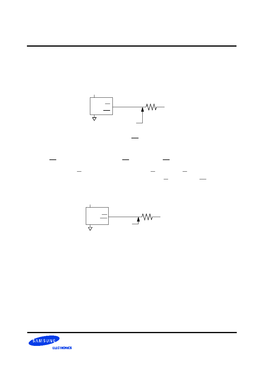
1. DDR2 SDRAM AC timing reference load
Figure 1 represents the timing reference load used in defining the relevant timing parameters of the part. It is not intended to be either a precise repre
sentation of the typical system environment or a depiction of the actual load presented by a production tester. System designers will use IBIS or other
simulation tools to correlate the timing reference load to a system environment. Manufacturers will correlate to their production test conditions (generally
a coaxial transmission line terminated at the tester electronics).
The output timing reference voltage level for single ended signals is the crosspoint with VTT. The output timing reference voltage level for differential
signals is the crosspoint of the true (e.g. DQS) and the complement (e.g. DQS) signal.
2. Slew Rate Measurement Levels
a) Output slew rate for falling and rising edges is measured between VTT - 250 mV and VTT + 250 mV for single ended signals. For differential signals
(e.g. DQS - DQS) output slew rate is measured between DQS - DQS = - 500 mV and DQS - DQS = + 500 mV. Output slew rate is guaranteed by
design, but is not necessarily tested on each device.
b) Input slew rate for single ended signals is measured from Vref(dc) to VIH(ac),min for rising edges and from Vref(dc) to VIL(ac),max for falling edges.
For differential signals (e.g. CK - CK) slew rate for rising edges is measured from CK - CK = - 250 mV to CK - CK = + 500 mV (+ 250 mV to - 500 mV
for falling edges).
c) VID is the magnitude of the difference between the input voltage on CK and the input voltage on CK, or between DQS and DQS for differential strobe.
3. DDR2 SDRAM output slew rate test load
Output slew rate is characterized under the test conditions as shown in Figure 2.
VDDQ
DUT
DQ
DQS
Output
VTT = VDDQ/2
25
Timing
reference
point
Figure 1 - AC Timing Reference Load
RDQS
VDDQ
DUT
DQ
DQS, DQS
RDQS, RDQS
Output
VTT = VDDQ/2
25
Test point
Figure 2 - Slew Rate Test Load
相关PDF资料 |
PDF描述 |
|---|---|
| K5A3240YT | Multi-Chip Package MEMORY 32M Bit (4Mx8/2Mx16) Dual Bank NOR Flash Memory / 4M(512Kx8/256Kx16) Full CMOS SRAM |
| K6R1004C1C | 256Kx4 Bit (with OE) High-Speed CMOS Static RAM(5.0V Operating). |
| K6R1004C1C-I | 256Kx4 Bit (with OE) High-Speed CMOS Static RAM(5.0V Operating). |
| K6R1004C1C-I10 | 256Kx4 Bit (with OE) High-Speed CMOS Static RAM(5.0V Operating). |
| K6R1004C1C-I12 | 256Kx4 Bit (with OE) High-Speed CMOS Static RAM(5.0V Operating). |
相关代理商/技术参数 |
参数描述 |
|---|---|
| K4T56163QN | 制造商:SAMSUNG 制造商全称:Samsung semiconductor 功能描述:Consumer Memory |
| K4T56163QN-HCE6000 | 制造商:Samsung SDI 功能描述:DRAM Chip DDR2 SDRAM 256M-Bit 16Mx16 1.8V 84-Pin FBGA Tray |
| K4T56163QN-HCE6T00 | 制造商:Samsung SDI 功能描述: |
| K4T56163QN-ZCE6T00 | 制造商:Samsung 功能描述:256 SDRAM X16 - Tape and Reel |
| K4T56163QN-ZCE7000 | 制造商:Samsung 功能描述:DDR2 SDRAM 32MX16 47H32M16 PBF FBGA 1.8V PLASTIC 512M - Trays |
发布紧急采购,3分钟左右您将得到回复。