- 您现在的位置:买卖IC网 > PDF目录224103 > K4T56163QI-ZLD50 16M X 16 SYNCHRONOUS DRAM, 0.5 ns, PBGA84 PDF资料下载
参数资料
| 型号: | K4T56163QI-ZLD50 |
| 元件分类: | DRAM |
| 英文描述: | 16M X 16 SYNCHRONOUS DRAM, 0.5 ns, PBGA84 |
| 封装: | ROHS COMPLIANT, FBGA-84 |
| 文件页数: | 34/42页 |
| 文件大小: | 727K |
| 代理商: | K4T56163QI-ZLD50 |
第1页第2页第3页第4页第5页第6页第7页第8页第9页第10页第11页第12页第13页第14页第15页第16页第17页第18页第19页第20页第21页第22页第23页第24页第25页第26页第27页第28页第29页第30页第31页第32页第33页当前第34页第35页第36页第37页第38页第39页第40页第41页第42页
Rev. 1.0 October 2007
DDR2 SDRAM
K4T56163QI
4 of 42
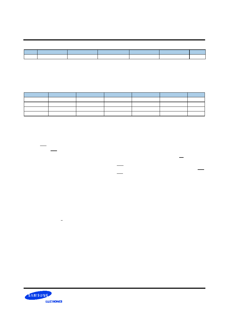
Speed
DDR2-800 5-5-5
DDR2-800 6-6-6
DDR2-667 5-5-5
DDR2-533 4-4-4
DDR2-400 3-3-3
Units
CAS Latency
5
6
5
43
tCK
tRCD(min)
12.5
15
ns
tRP(min)
12.5
15
ns
tRC(min)
57.5
60
55
ns
Note :
1. Speed bin is in order of CL-tRCD-tRP
2. RoHS Compliant
Org.
DDR2-800 5-5-5
DDR2-800 6-6-6
DDR2-667 5-5-5
DDR2-533 4-4-4
DDR2-400 3-3-3
Package
16Mx16
K4T56163QI-ZC(L)E7
K4T56163QI-ZC(L)F7
K4T56163QI-ZC(L)E6
K4T56163QI-ZC(L)D5
K4T56163QI-ZC(L)CC
84 FBGA
JEDEC standard 1.8V ± 0.1V Power Supply
VDDQ = 1.8V ± 0.1V
200 MHz fCK for 400Mb/sec/pin, 267MHz fCK for 533Mb/sec/
pin, 333MHz fCK for 667Mb/sec/pin, 400MHz fCK for 800Mb/
sec/pin
4 Banks
Posted CAS
Programmable CAS Latency: 3, 4, 5, 6
Programmable Additive Latency: 0, 1 , 2 , 3, 4 , 5
Write Latency(WL) = Read Latency(RL) -1
Burst Length: 4 , 8(Interleave/nibble sequential)
Programmable Sequential / Interleave Burst Mode
Bi-directional Differential Data-Strobe (Single-ended data-
strobe is an optional feature)
Off-Chip Driver(OCD) Impedance Adjustment
On Die Termination
Special Function Support
-PASR(Partial Array Self Refresh)
-50ohm ODT
-High Temperature Self-Refresh rate enable
Average Refresh Period 7.8us at lower than TCASE 85°C,
3.9us at 85
°C < TCASE < 95 °C
All of Lead-free products are compliant for RoHS
The 256Mb DDR2 SDRAM is organized as a 4Mbit x 16 I/Os x 4
banks device. This synchronous device achieves high speed dou-
ble-data-rate transfer rates of up to 800Mb/sec/pin (DDR2-800) for
general applications.
The chip is designed to comply with the following key DDR2
SDRAM features such as posted CAS with additive latency, write
latency = read latency -1, Off-Chip Driver(OCD) impedance
adjustment and On Die Termination.
All of the control and address inputs are synchronized with a pair
of externally supplied differential clocks. Inputs are latched at the
crosspoint of differential clocks (CK rising and CK falling). All I/Os
are synchronized with a pair of bidirectional strobes (DQS and
DQS) in a source synchronous fashion. The address bus is used
to convey row, column, and bank address information in a RAS/
CAS multiplexing style. For example, 256Mb(x16) device receive
13/9/2 addressing.
The 256Mb DDR2 device operates with a single 1.8V ± 0.1V
power supply and 1.8V ± 0.1V VDDQ.
The 256Mb DDR2 device is available in 84ball FBGAs(x16).
Note : The functionality described and the timing specifications included in
this data sheet are for the DLL Enabled mode of operation.
Note : This data sheet is an abstract of full DDR2 specification and does not cover the common features which are described in “Samsung’s DDR2
SDRAM Device Operation & Timing Diagram”
1.0 Ordering Information
2.0 Key Features
相关PDF资料 |
PDF描述 |
|---|---|
| K5A3240YT | Multi-Chip Package MEMORY 32M Bit (4Mx8/2Mx16) Dual Bank NOR Flash Memory / 4M(512Kx8/256Kx16) Full CMOS SRAM |
| K6R1004C1C | 256Kx4 Bit (with OE) High-Speed CMOS Static RAM(5.0V Operating). |
| K6R1004C1C-I | 256Kx4 Bit (with OE) High-Speed CMOS Static RAM(5.0V Operating). |
| K6R1004C1C-I10 | 256Kx4 Bit (with OE) High-Speed CMOS Static RAM(5.0V Operating). |
| K6R1004C1C-I12 | 256Kx4 Bit (with OE) High-Speed CMOS Static RAM(5.0V Operating). |
相关代理商/技术参数 |
参数描述 |
|---|---|
| K4T56163QN | 制造商:SAMSUNG 制造商全称:Samsung semiconductor 功能描述:Consumer Memory |
| K4T56163QN-HCE6000 | 制造商:Samsung SDI 功能描述:DRAM Chip DDR2 SDRAM 256M-Bit 16Mx16 1.8V 84-Pin FBGA Tray |
| K4T56163QN-HCE6T00 | 制造商:Samsung SDI 功能描述: |
| K4T56163QN-ZCE6T00 | 制造商:Samsung 功能描述:256 SDRAM X16 - Tape and Reel |
| K4T56163QN-ZCE7000 | 制造商:Samsung 功能描述:DDR2 SDRAM 32MX16 47H32M16 PBF FBGA 1.8V PLASTIC 512M - Trays |
发布紧急采购,3分钟左右您将得到回复。