- 您现在的位置:买卖IC网 > PDF目录224103 > K4T56163QI-ZLD50 16M X 16 SYNCHRONOUS DRAM, 0.5 ns, PBGA84 PDF资料下载
参数资料
| 型号: | K4T56163QI-ZLD50 |
| 元件分类: | DRAM |
| 英文描述: | 16M X 16 SYNCHRONOUS DRAM, 0.5 ns, PBGA84 |
| 封装: | ROHS COMPLIANT, FBGA-84 |
| 文件页数: | 33/42页 |
| 文件大小: | 727K |
| 代理商: | K4T56163QI-ZLD50 |
第1页第2页第3页第4页第5页第6页第7页第8页第9页第10页第11页第12页第13页第14页第15页第16页第17页第18页第19页第20页第21页第22页第23页第24页第25页第26页第27页第28页第29页第30页第31页第32页当前第33页第34页第35页第36页第37页第38页第39页第40页第41页第42页
Rev. 1.0 October 2007
DDR2 SDRAM
K4T56163QI
39 of 42
24. tWTR is at lease two clocks (2 x tCK or 2 x nCK) independent of operation frequency.
25. Input waveform timing with single-ended data strobe enabled MR[bit10] = 1, is referenced from the input signal crossing at the VIH(ac) level to the
single-ended data strobe crossing VIH/L(dc) at the start of its transition for a rising signal, and from the input signal crossing at the VIL(ac) level to the
single-ended data strobe crossing VIH/L(dc) at the start of its transition for a falling signal applied to the device under test. The DQS signal must be
monotonic between Vil(dc)max and Vih(dc)min.
26. Input waveform timing with single-ended data strobe enabled MR[bit10] = 1, is referenced from the input signal crossing at the VIH(dc) level to the
single-ended data strobe crossing VIH/L(ac) at the end of its transition for a rising signal, and from the input signal crossing at the VIL(dc) level to the
single-ended data strobe crossing VIH/L(ac) at the end of its transition for a falling signal applied to the device under test. The DQS signal must be
monotonic between Vil(dc)max and Vih(dc)min.
27. tCKEmin of 3 clocks means CKE must be registered on three consecutive positive clock edges. CKE must remain at the valid input level the entire
time it takes to achieve the 3 clocks of registration. Thus, after any CKE transition, CKE may not transition from its valid level during the time period
of tIS + 2 x tCK + tIH.
28. If tDS or tDH is violated, data corruption may occur and the data must be re-written with valid data before a valid READ can be executed.
29. These parameters are measured from a command/address signal (CKE, CS, RAS, CAS, WE, ODT, BA0, A0, A1, etc.) transition edge to its respec-
tive clock signal (CK/CK) crossing. The spec values are not affected by the amount of clock jitter applied (i.e. tJIT(per), tJIT(cc), etc.), as the setup
and hold are relative to the clock signal crossing that latches the command/address. That is, these parameters should be met whether clock jitter is
present or not.
30. These parameters are measured from a data strobe signal ((L/U/R)DQS/DQS) crossing to its respective clock signal (CK/CK) crossing. The spec val-
ues are not affected by the amount of clock jitter applied (i.e. tJIT(per), tJIT(cc), etc.), as these are relative to the clock signal crossing. That is, these
parameters should be met whether clock jitter is present or not.
31. These parameters are measured from a data signal ((L/U)DM, (L/U)DQ0, (L/U)DQ1, etc.) transition edge to its respective data strobe signal ((L/U/
R)DQS/DQS) crossing.
32. For these parameters, the DDR2 SDRAM device is characterized and verified to support tnPARAM = RU{tPARAM / tCK(avg)}, which is in clock
cycles, assuming all input clock jitter specifications are satisfied.
For example, the device will support tnRP = RU{tRP / tCK(avg)}, which is in clock cycles, if all input clock jitter specifications are met. This means:
For DDR2-667 5-5-5, of which tRP = 15ns, the device will support tnRP = RU{tRP / tCK(avg)} = 5, i.e. as long as the input clock jitter specifications
are met, Precharge command at Tm and Active command at Tm+5 is valid even if (Tm+5 - Tm) is less than 15ns due to input clock jitter.
33. tDAL [nCK] = WR [nCK] + tnRP [nCK] = WR + RU {tRP [ps] / tCK(avg) [ps] }, where WR is the value programmed in the mode register set.
34. New units, ’tCK(avg)’ and ’nCK’, are introduced in DDR2-667 and DDR2-800. Unit ’tCK(avg)’ represents the actual tCK(avg) of the input clock under
operation. Unit ’nCK’ represents one clock cycle of the input clock, counting the actual clock edges.
Note that in DDR2-400 and DDR2-533, ’tCK’ is used for both concepts.
ex) tXP = 2 [nCK] means; if Power Down exit is registered at Tm, an Active command may be registered at Tm+2, even if (Tm+2 - Tm) is 2 x
tCK(avg) + tERR(2per),min.
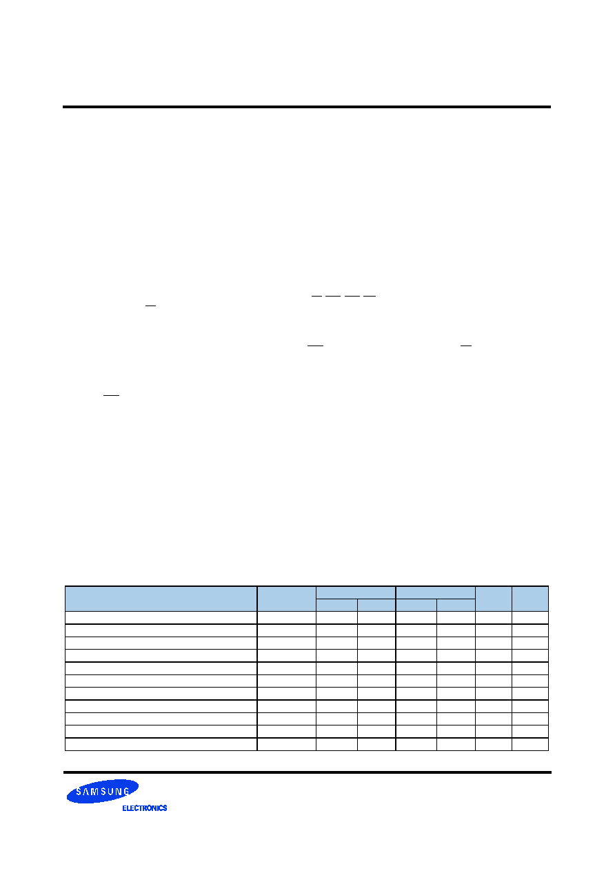
35. Input clock jitter spec parameter. These parameters and the ones in the table below are referred to as 'input clock jitter spec parameters' and these
parameters apply to DDR2-667 and DDR2-800 only. The jitter specified is a random jitter meeting a Gaussian distribution.
Parameter
Symbol
DDR2-667
DDR2-800
units
Notes
Min
Max
Min
Max
Clock period jitter
tJIT(per)
-125
125
-100
100
ps
35
Clock period jitter during DLL locking period
tJIT(per,lck)
-100
100
-80
80
ps
35
Cycle to cycle clock period jitter
tJIT(cc)
-250
250
-200
200
ps
35
Cycle to cycle clock period jitter during DLL locking period
tJIT(cc,lck)
-200
200
-160
160
ps
35
Cumulative error across 2 cycles
tERR(2per)
-175
175
-150
150
ps
35
Cumulative error across 3 cycles
tERR(3per)
-225
225
-175
175
ps
35
Cumulative error across 4 cycles
tERR(4per)
-250
250
-200
200
ps
35
Cumulative error across 5 cycles
tERR(5per)
-250
250
-200
200
ps
35
Cumulative error across n cycles, n = 6 ... 10, inclusive
tERR(6-10per)
-350
350
-300
300
ps
35
Cumulative error across n cycles, n = 11 ... 50, inclusive
tERR(11-50per)
-450
450
-450
450
ps
35
Duty cycle jitter
tJIT(duty)
-125
125
-100
100
ps
35
相关PDF资料 |
PDF描述 |
|---|---|
| K5A3240YT | Multi-Chip Package MEMORY 32M Bit (4Mx8/2Mx16) Dual Bank NOR Flash Memory / 4M(512Kx8/256Kx16) Full CMOS SRAM |
| K6R1004C1C | 256Kx4 Bit (with OE) High-Speed CMOS Static RAM(5.0V Operating). |
| K6R1004C1C-I | 256Kx4 Bit (with OE) High-Speed CMOS Static RAM(5.0V Operating). |
| K6R1004C1C-I10 | 256Kx4 Bit (with OE) High-Speed CMOS Static RAM(5.0V Operating). |
| K6R1004C1C-I12 | 256Kx4 Bit (with OE) High-Speed CMOS Static RAM(5.0V Operating). |
相关代理商/技术参数 |
参数描述 |
|---|---|
| K4T56163QN | 制造商:SAMSUNG 制造商全称:Samsung semiconductor 功能描述:Consumer Memory |
| K4T56163QN-HCE6000 | 制造商:Samsung SDI 功能描述:DRAM Chip DDR2 SDRAM 256M-Bit 16Mx16 1.8V 84-Pin FBGA Tray |
| K4T56163QN-HCE6T00 | 制造商:Samsung SDI 功能描述: |
| K4T56163QN-ZCE6T00 | 制造商:Samsung 功能描述:256 SDRAM X16 - Tape and Reel |
| K4T56163QN-ZCE7000 | 制造商:Samsung 功能描述:DDR2 SDRAM 32MX16 47H32M16 PBF FBGA 1.8V PLASTIC 512M - Trays |
发布紧急采购,3分钟左右您将得到回复。