- 您现在的位置:买卖IC网 > PDF目录187165 > MT46V32M8P-75ELIT:G 64M X 8 DDR DRAM, 0.75 ns, PDSO66 PDF资料下载
参数资料
| 型号: | MT46V32M8P-75ELIT:G |
| 元件分类: | DRAM |
| 英文描述: | 64M X 8 DDR DRAM, 0.75 ns, PDSO66 |
| 封装: | 0.40 INCH, LEAD FREE,PLASTIC, TSOP-66 |
| 文件页数: | 20/93页 |
| 文件大小: | 3632K |
第1页第2页第3页第4页第5页第6页第7页第8页第9页第10页第11页第12页第13页第14页第15页第16页第17页第18页第19页当前第20页第21页第22页第23页第24页第25页第26页第27页第28页第29页第30页第31页第32页第33页第34页第35页第36页第37页第38页第39页第40页第41页第42页第43页第44页第45页第46页第47页第48页第49页第50页第51页第52页第53页第54页第55页第56页第57页第58页第59页第60页第61页第62页第63页第64页第65页第66页第67页第68页第69页第70页第71页第72页第73页第74页第75页第76页第77页第78页第79页第80页第81页第82页第83页第84页第85页第86页第87页第88页第89页第90页第91页第92页第93页
PDF: 09005aef80768abb/Source: 09005aef82a95a3a
Micron Technology, Inc., reserves the right to change products or specifications without notice.
DDR_x4x8x16_Core2.fm - 256Mb DDR: Rev. O, Core DDR: Rev. B 1/09 EN
25
2003 Micron Technology, Inc. All rights reserved.
256Mb: x4, x8, x16 DDR SDRAM
Electrical Specifications – DC and AC
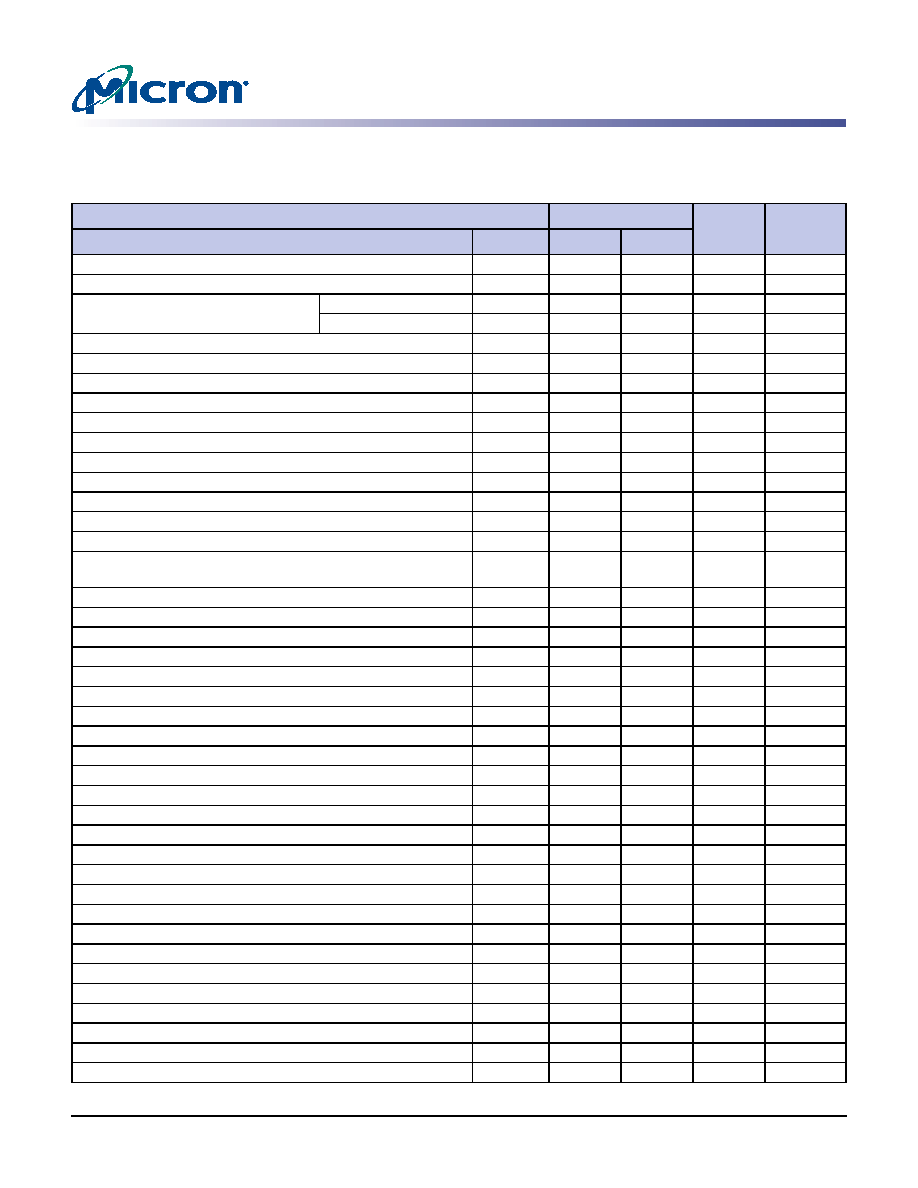
Table 19:
Electrical Characteristics and Recommended AC Operating Conditions (-6)
0°C
≤ T
A ≤ +70°C; VDDQ = +2.5V ±0.2V, VDD = +2.5V ±0.2V
AC Characteristics
-6 (FBGA)
Units
Notes
Parameter
Symbol
Min
Max
Access window of DQ from CK/CK#
tAC
–0.70
+0.70
ns
CK high-level width
tCH
0.45
0.55
tCK
Clock cycle time
CL = 2.5
tCK (2.5)
6
13
ns
CL = 2
tCK (2)
7.5
13
ns
CK low-level width
tCL
0.45
0.55
tCK
DQ and DM input hold time relative to DQS
tDH
0.45
–
ns
DQ and DM input pulse width (for each input)
tDIPW
1.75
–
ns
Access window of DQS from CK/CK#
tDQSCK
–0.6
+0.6
ns
DQS input high pulse width
tDQSH
0.35
–
tCK
DQS input low pulse width
tDQSL
0.35
–
tCK
DQS–DQ skew, DQS to last DQ valid, per group, per access
tDQSQ
–
0.4
ns
WRITE command to first DQS latching transition
tDQSS
0.75
1.25
tCK
DQ and DM input setup time relative to DQS
tDS
0.45
–
ns
DQS falling edge from CK rising - hold time
tDSH
0.2
–
tCK
DQS falling edge to CK rising - setup time
tDSS
0.2
–
tCK
Half-clock period
tHP
tCH,
tCL
–ns
Data-out High-Z window from CK/CK#
tHZ
–
+0.7
ns
Address and control input hold time (fast slew rate)
tIH
F
0.75
–
ns
Address and control input hold time (slow slew rate)
tIH
S
0.8
–
ns
Address and control input pulse width (for each input)
tIPW
2.2
–
ns
Address and control input setup time (fast slew rate)
tIS
F
0.75
–
ns
Address and control input setup time (slow slew rate)
tIS
S
0.8
–
ns
Data-out Low-Z window from CK/CK#
tLZ
–0.7
–
ns
LOAD MODE REGISTER command cycle time
tMRD
12
–
ns
DQ-DQS hold, DQS to first DQ to go non-valid, per access
tQH
tHP -tQHS
–
ns
Data hold skew factor
tQHS
–
0.50
ns
ACTIVE-to-READ with auto precharge command
tRAP
15
–
ns
ACTIVE-to-PRECHARGE command
tRAS
42
70,000
ns
ACTIVE-to-ACTIVE/AUTO REFRESH command period
tRC
60
–
ns
ACTIVE-to-READ or WRITE delay
tRCD
15
–
ns
REFRESH-to-REFRESH command interval
tREFC
–
70.3
s
REFRESH-to-REFRESH command interval (Automotive)
tREFC
AT
–
17.55
s
Average periodic refresh interval
tREFI
–
7.8
s
Average periodic refresh interval (Automotive)
tREFI
AT
–1.95
s
AUTO REFRESH command period
tRFC
72
–
ns
PRECHARGE command period
tRP
15
–
ns
DQS read preamble
tRPRE
0.9
1.1
tCK
DQS read postamble
tRPST
0.4
0.6
tCK
ACTIVE bank a to ACTIVE bank b command
tRRD
12
–
ns
Terminating voltage delay to VSS
tVTD
0
–
ns
DQS write preamble
tWPRE
0.25
–
tCK
相关PDF资料 |
PDF描述 |
|---|---|
| MT47H128M4CC-3:B | 128M X 4 DDR DRAM, 0.45 ns, PBGA84 |
| MT47H32M16HR-37EAT:G | 32M X 16 DDR DRAM, 0.5 ns, PBGA84 |
| MT47H64M16BT-3ELIT:A | 64M X 16 DDR DRAM, 0.45 ns, PBGA92 |
| MT47H64M8B6-3ELAT:D | DDR DRAM, PBGA60 |
| MT48H32M16LFCJ-8 | 32M X 16 SYNCHRONOUS DRAM, 7 ns, PBGA54 |
相关代理商/技术参数 |
参数描述 |
|---|---|
| MT46V32M8T66ADC1 | 制造商:Micron Technology Inc 功能描述:32MX8 DDR SDRAM DIE-COM COMMERCIAL 2.5V - Trays |
| MT46V32M8TG-5B/G | 制造商:Micron Technology Inc 功能描述:DRAM Chip DDR SDRAM 256M-Bit 32Mx8 2.6V 66-Pin TSOP Tray |
发布紧急采购,3分钟左右您将得到回复。