- 您现在的位置:买卖IC网 > PDF目录187165 > MT46V32M8P-75ELIT:G 64M X 8 DDR DRAM, 0.75 ns, PDSO66 PDF资料下载
参数资料
| 型号: | MT46V32M8P-75ELIT:G |
| 元件分类: | DRAM |
| 英文描述: | 64M X 8 DDR DRAM, 0.75 ns, PDSO66 |
| 封装: | 0.40 INCH, LEAD FREE,PLASTIC, TSOP-66 |
| 文件页数: | 59/93页 |
| 文件大小: | 3632K |
第1页第2页第3页第4页第5页第6页第7页第8页第9页第10页第11页第12页第13页第14页第15页第16页第17页第18页第19页第20页第21页第22页第23页第24页第25页第26页第27页第28页第29页第30页第31页第32页第33页第34页第35页第36页第37页第38页第39页第40页第41页第42页第43页第44页第45页第46页第47页第48页第49页第50页第51页第52页第53页第54页第55页第56页第57页第58页当前第59页第60页第61页第62页第63页第64页第65页第66页第67页第68页第69页第70页第71页第72页第73页第74页第75页第76页第77页第78页第79页第80页第81页第82页第83页第84页第85页第86页第87页第88页第89页第90页第91页第92页第93页
PDF: 09005aef80768abb/Source: 09005aef82a95a3a
Micron Technology, Inc., reserves the right to change products or specifications without notice.
DDR_x4x8x16_Core2.fm - 256Mb DDR: Rev. O, Core DDR: Rev. B 1/09 EN
60
2003 Micron Technology, Inc. All rights reserved.
256Mb: x4, x8, x16 DDR SDRAM
Operations
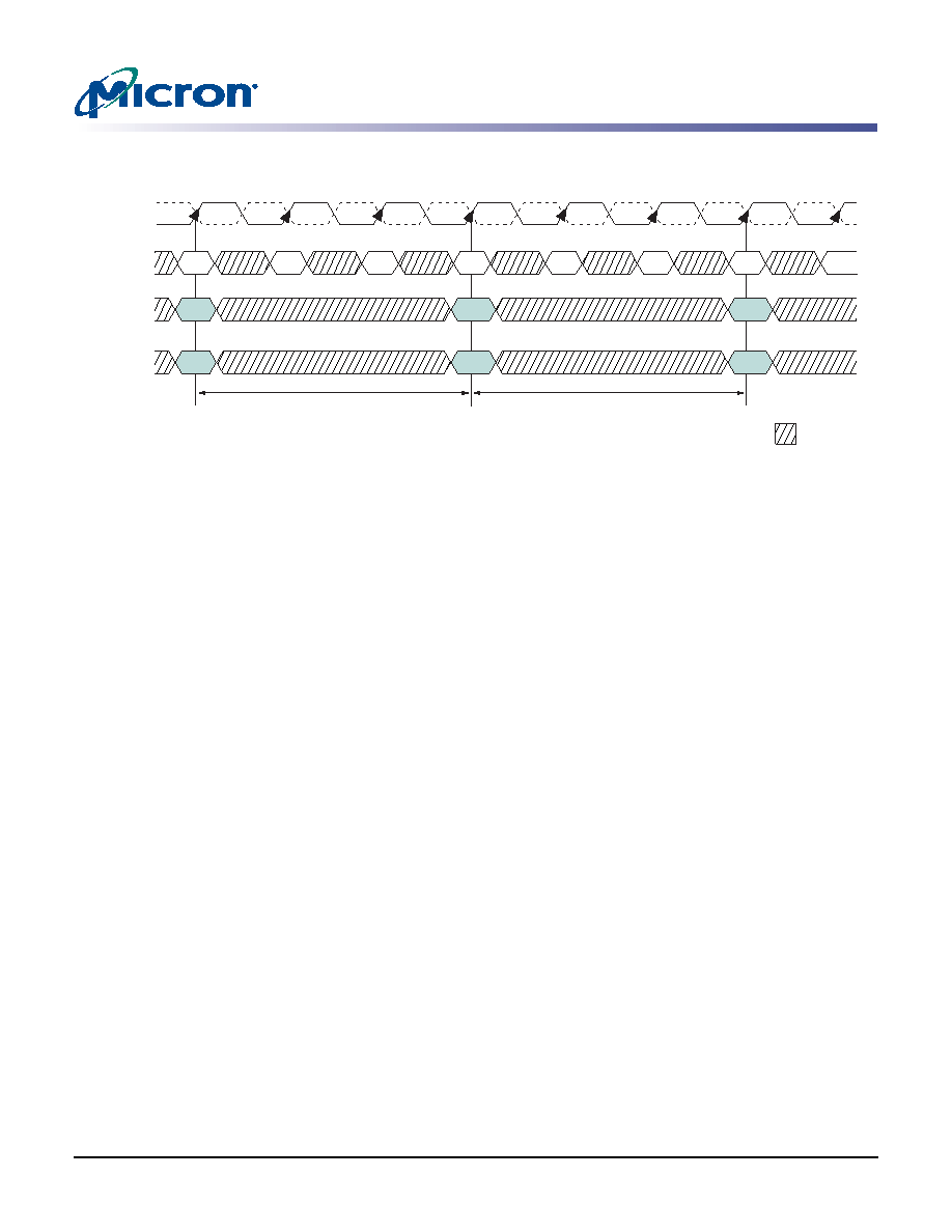
Figure 26:
Example: Meeting tRCD (tRRD) MIN When 2 < tRCD (tRRD) MIN/tCK
≤ 3
READ
During the READ command, the value on input A10 determines whether or not auto
precharge is used. If auto precharge is selected, the row being accessed will be
precharged at the end of the READ burst; if auto precharge is not selected, the row will
remain open for subsequent accesses.
Note:
For the READ commands used in the following illustrations, auto precharge is dis-
abled.
During READ bursts, the valid data-out element from the starting column address will
be available following the CL after the READ command. Each subsequent data-out
element will be valid nominally at the next positive or negative clock edge (that is, at the
next crossing of CK and CK#). Figure 27 on page 62 shows the general timing for each
possible CL setting. DQS is driven by the DDR SDRAM along with output data. The
initial LOW state on DQS is known as the read preamble; the LOW state coincident with
the last data-out element is known as the read postamble.
Upon completion of a burst, assuming no other commands have been initiated, the DQ
will go High-Z. Detailed explanations of tDQSQ (valid data-out skew), tQH (data-out
window hold), and the valid data window are depicted in Figure 35 on page 70 and
tAC (data-out transition skew to CK) are depicted in Figure 37 on page 72.
Data from any READ burst may be concatenated or truncated with data from a subse-
quent READ command. In either case, a continuous flow of data can be maintained. The
first data element from the new burst follows either the last element of a completed
burst or the last desired data element of a longer burst which is being truncated. The
new READ command should be issued x cycles after the first READ command, where x
equals the number of desired data element pairs (pairs are required by the 2n-prefetch
architecture). This is shown in Figure 28 on page 63. A READ command can be initiated
on any clock cycle following a previous READ command. Nonconsecutive read data is
illustrated in Figure 29 on page 64. Full-speed random read accesses within a page (or
pages) can be performed, as shown in Figure 30 on page 65.
Command
BA0, BA1
ACTACT
NOP
tRRD
tRCD
CK
CK#
Bank x
Bank y
Address
Row
NOP
RD/WR
NOP
Bank y
Col
NOP
T0
T1
T2
T3
T4
T5
T6
T7
Don’t Care
NOP
相关PDF资料 |
PDF描述 |
|---|---|
| MT47H128M4CC-3:B | 128M X 4 DDR DRAM, 0.45 ns, PBGA84 |
| MT47H32M16HR-37EAT:G | 32M X 16 DDR DRAM, 0.5 ns, PBGA84 |
| MT47H64M16BT-3ELIT:A | 64M X 16 DDR DRAM, 0.45 ns, PBGA92 |
| MT47H64M8B6-3ELAT:D | DDR DRAM, PBGA60 |
| MT48H32M16LFCJ-8 | 32M X 16 SYNCHRONOUS DRAM, 7 ns, PBGA54 |
相关代理商/技术参数 |
参数描述 |
|---|---|
| MT46V32M8T66ADC1 | 制造商:Micron Technology Inc 功能描述:32MX8 DDR SDRAM DIE-COM COMMERCIAL 2.5V - Trays |
| MT46V32M8TG-5B/G | 制造商:Micron Technology Inc 功能描述:DRAM Chip DDR SDRAM 256M-Bit 32Mx8 2.6V 66-Pin TSOP Tray |
发布紧急采购,3分钟左右您将得到回复。