- 您现在的位置:买卖IC网 > PDF目录187165 > MT46V32M8P-75ELIT:G 64M X 8 DDR DRAM, 0.75 ns, PDSO66 PDF资料下载
参数资料
| 型号: | MT46V32M8P-75ELIT:G |
| 元件分类: | DRAM |
| 英文描述: | 64M X 8 DDR DRAM, 0.75 ns, PDSO66 |
| 封装: | 0.40 INCH, LEAD FREE,PLASTIC, TSOP-66 |
| 文件页数: | 68/93页 |
| 文件大小: | 3632K |
第1页第2页第3页第4页第5页第6页第7页第8页第9页第10页第11页第12页第13页第14页第15页第16页第17页第18页第19页第20页第21页第22页第23页第24页第25页第26页第27页第28页第29页第30页第31页第32页第33页第34页第35页第36页第37页第38页第39页第40页第41页第42页第43页第44页第45页第46页第47页第48页第49页第50页第51页第52页第53页第54页第55页第56页第57页第58页第59页第60页第61页第62页第63页第64页第65页第66页第67页当前第68页第69页第70页第71页第72页第73页第74页第75页第76页第77页第78页第79页第80页第81页第82页第83页第84页第85页第86页第87页第88页第89页第90页第91页第92页第93页
PDF: 09005aef80768abb/Source: 09005aef82a95a3a
Micron Technology, Inc., reserves the right to change products or specifications without notice.
DDR_x4x8x16_Core2.fm - 256Mb DDR: Rev. O, Core DDR: Rev. B 1/09 EN
68
2003 Micron Technology, Inc. All rights reserved.
256Mb: x4, x8, x16 DDR SDRAM
Operations
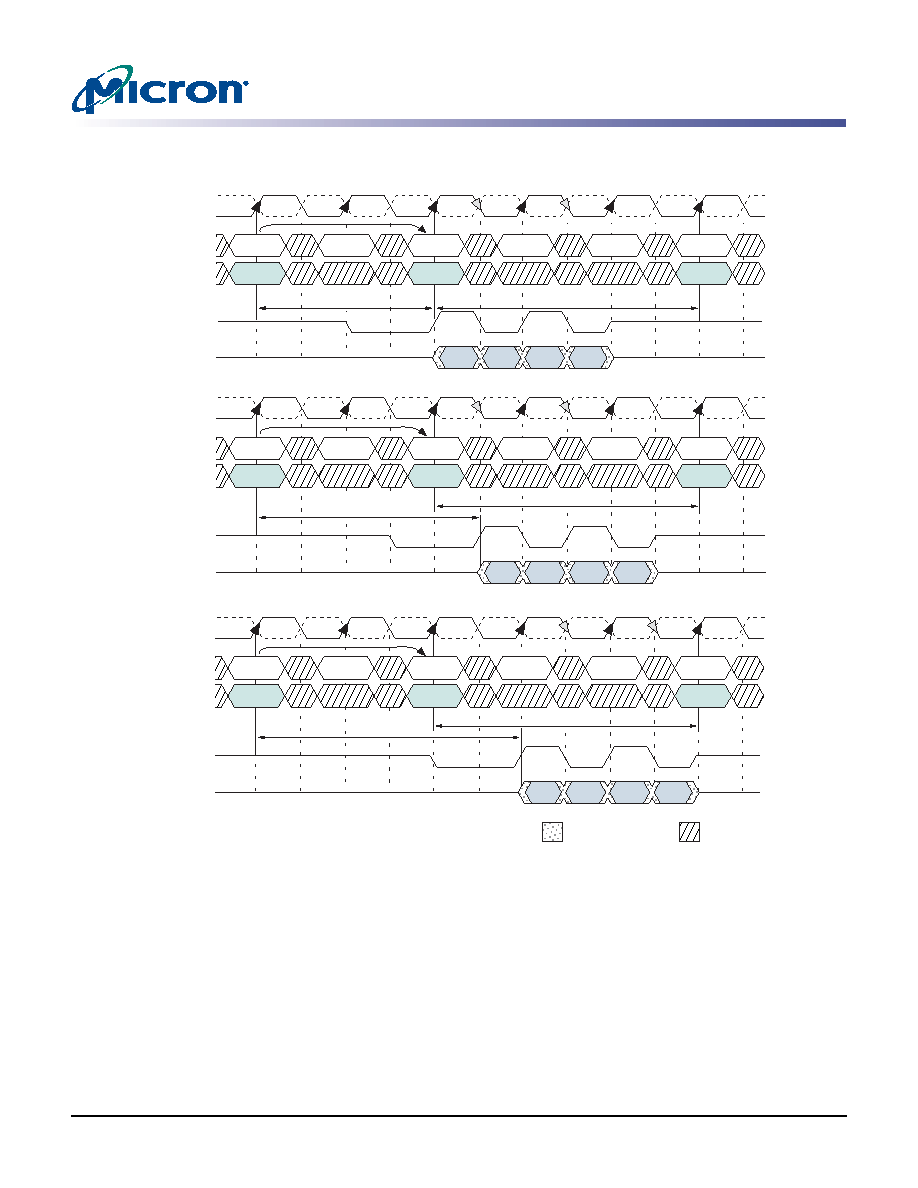
Figure 33:
READ-to-PRECHARGE
Notes:
1. Provided tRAS (MIN) is met, a READ command with auto precharge enabled would cause a
precharge to be performed at x number of clock cycles after the READ command, where
x =BL/2.
2. DO n = data-out from column n.
3. BL = 4 or an interrupted burst of 8.
4. Three subsequent elements of data-out appear in the programmed order following DO n.
5. Shown with nominal tAC, tDQSCK, and tDQSQ.
6. READ-to-PRECHARGE equals two clocks, which allows two data pairs of data-out; it is also
assumed that tRAS (MIN) is met.
7. An ACTIVE command to the same bank is only allowed if tRC (MIN) is met.
READ
NOP
PRE
NOP
ACT
Bank a,
Col n
Bank a,
(a or all)
Bank a,
Row
READ
NOP
PRE
NOP
ACT
Bank a,
Col n
CL = 2
tRP
CL = 2.5
DO
n
DO
n
T0
T1
T2
T3
T2n
T3n
T4
T5
T0
T1
T2
T3
T2n
T3n
T4
T5
Bank a,
(a or all)
Bank a,
Row
READ
NOP
PRE
NOP
ACT
Bank a,
Col n
tRP
CL = 3
DO
n
T0
T1
T2
T3
T4n
T3n
T4
T5
Bank a,
(a or all)
Bank a,
Row
Command
Address
DQS
DQ
CK#
CK
Command
Address
DQS
DQ
CK#
CK
Command
Address
DQS
DQ
CK#
CK
Transitioning Data
Don’t Care
相关PDF资料 |
PDF描述 |
|---|---|
| MT47H128M4CC-3:B | 128M X 4 DDR DRAM, 0.45 ns, PBGA84 |
| MT47H32M16HR-37EAT:G | 32M X 16 DDR DRAM, 0.5 ns, PBGA84 |
| MT47H64M16BT-3ELIT:A | 64M X 16 DDR DRAM, 0.45 ns, PBGA92 |
| MT47H64M8B6-3ELAT:D | DDR DRAM, PBGA60 |
| MT48H32M16LFCJ-8 | 32M X 16 SYNCHRONOUS DRAM, 7 ns, PBGA54 |
相关代理商/技术参数 |
参数描述 |
|---|---|
| MT46V32M8T66ADC1 | 制造商:Micron Technology Inc 功能描述:32MX8 DDR SDRAM DIE-COM COMMERCIAL 2.5V - Trays |
| MT46V32M8TG-5B/G | 制造商:Micron Technology Inc 功能描述:DRAM Chip DDR SDRAM 256M-Bit 32Mx8 2.6V 66-Pin TSOP Tray |
发布紧急采购,3分钟左右您将得到回复。