- 您现在的位置:买卖IC网 > Datasheet目录484 > NOIH2SM1000S-HHC (ON Semiconductor)IC SPACE IMAGE SENSOR 84-JLCC Datasheet资料下载
参数资料
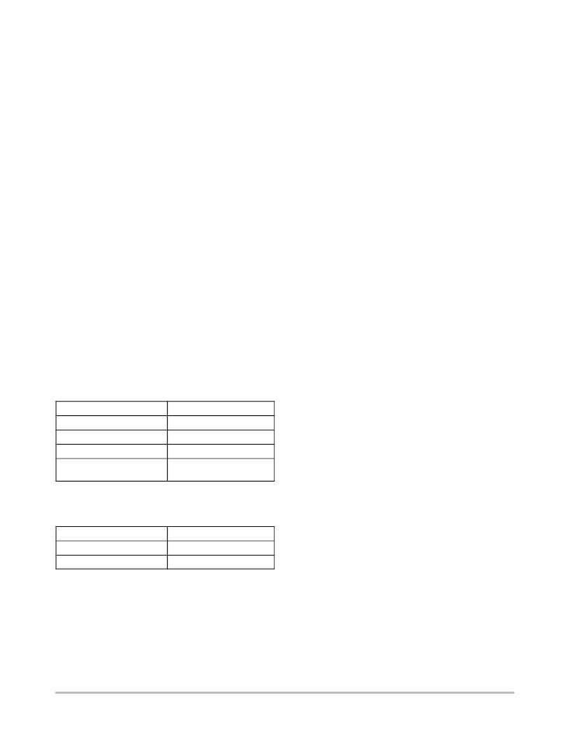
| 型号: | NOIH2SM1000S-HHC |
| 厂商: | ON Semiconductor |
| 文件页数: | 3/67页 |
| 文件大小: | 0K |
| 描述: | IC SPACE IMAGE SENSOR 84-JLCC |
| 标准包装: | 1 |
| 系列: | HAS2 |
| 象素大小: | 18µm x 18µm |
| 有源象素阵列: | 1024H x 1024V |
| 电源电压: | 3.3V |
| 类型: | CMOS 成像 |
| 封装/外壳: | * |
| 供应商设备封装: | * |
| 包装: | * |
| 其它名称: | CYIH1SM1000AA-HHCS CYIH1SM1000AA-HHCS-ND |
第1页第2页当前第3页第4页第5页第6页第7页第8页第9页第10页第11页第12页第13页第14页第15页第16页第17页第18页第19页第20页第21页第22页第23页第24页第25页第26页第27页第28页第29页第30页第31页第32页第33页第34页第35页第36页第37页第38页第39页第40页第41页第42页第43页第44页第45页第46页第47页第48页第49页第50页第51页第52页第53页第54页第55页第56页第57页第58页第59页第60页第61页第62页第63页第64页第65页第66页第67页
�� �
�
�NOIH2SM1000A�
�DETAILED� INFORMATION�
�Deviations� from� Generic� Specification�
�Lot� acceptance� and� screening� are� based� on� ESCC� 9020�
�issue� 2.� See� Lot� Acceptance� and� Screening� on� page� 6� for�
�more� information.�
�Mechanical� Requirements�
�Dimension� Check�
�The� dimensions� of� the� components� specified� here� is�
�checked� and� must� comply� with� the� specifications� and� the�
�tolerances� indicated� in� Figure� 4� on� page� 25�
�Geometrical� Characteristics�
�The� geometrical� characteristics� of� the� components�
�specified� here� is� checked� and� must� comply� with� the�
�specifications� and� tolerances� given� in� Figure� 4� on� page� 25�
�and� Figure� 3� on� page� 10�
�Weight�
�The� maximum� weight� of� the� components� specified� here� is�
�specified� in� Table� 14� on� page� 10�
�Materials� and� Finishes�
�The� materials� and� finishes� is� as� specified� in� this� document.�
�Where� a� definite� material� is� not� specified,� a� material� which�
�enables� the� components� to� meet� the� performance�
�requirements� of� this� specification� must� be� used.� See� Note� 2.�
�Case�
�The� case� is� hermetically� sealed� and� must� have� a� ceramic�
�body� and� a� glass� window.�
�Table� 3.� CASE�
�Type� JLCC� ?� 84�
�Material� Black� Alumina� BA� ?� 914�
�Thermal� expansion� coefficient� 7.6� x� 10� ?� 6/K�
�Hermeticity� <� 5� x� 10� ?� 7� atms.� cm� 3� /s�
�Thermal� resistance� 3.633� °� C/W�
�(Junction� to� case)�
�Lead� Material� and� Finish�
�Table� 4.� LEAD� MATERIAL� AND� FINISH�
�The� anti� reflective� coating� has� a� reflection� coefficient� less�
�than� 1.3%� absolute� and� less� than� 0.8%� on� average,� over� a�
�bandwidth� from� 440� nm� to� 1100� nm.�
�Level� 2� versus� Level� 1� differences�
�HAS2� Level� 2� devices� are� differing� from� Level� 1� devices�
�in� Lot� Acceptance� and� Screening� on� page� 6�
�?� 100%� screening� is� applied� with� burn-in� limited� to� 168� h�
�instead� of� 240� h� as� for� Level� 1.�
�?� Assembly� process� is� based� on� ESA� qualified� process�
�(same� procedures� and� materials)�
�?� Devices� will� be� fully� tested� at� room� temperature,�
�electrical� testing� at� 85� degrees� is� limited� to� power�
�consumption� measurements� only.�
�?� X/Y� dye� placement� is� relaxed� to� +/-� 200� m� m.�
�?� Mismatching� between� odd� and� even� columns� in� Direct�
�Readout� is� allowed� but� shall� stay� in� the� limit� of�
�127� LSB.�
�?� The� defect� and� particles� specification� will� be� the� same�
�as� for� the� Engineering� Model� -� NOIH2SM1000A-HHC�
�–� with� the� exception� of� the� defective� columns� which� are�
�not� allowed� in� the� Level� 2� devices.� Refer� to� Table� 10�
�“Type� Variant� Summary”� on� page� 9.�
�?� Endurance� testing� during� wafer� LAT� is� limited� to� a�
�1000� h� burn� in� instead� of� 2000� h� and� will� be� performed�
�on� 3� un-� screened� parts� instead� of� 6.�
�?� Prior� to� endurance� testing� and� total� dose� testing,� a�
�stabilization� bake� of� 48� hrs,� followed� by� a� 168� hrs�
�burn-in,� shall� be� performed.�
�?� During� wafer� LAT,� the� Electro-optical� measurements� is�
�limited� on� 2� parts� (1� from� endurance� testing� and� 1� from�
�radiation� testing)� instead� of� 6.�
�?� For� each� assembly� batch� (manufacturing-lot),� 2�
�screened� devices� will� be� made� available� for� a� DPA� test.�
�An� assembly� batch� is� defined� as� a� group� of� parts� which�
�have� been� assembled� within� a� time� window� of� less� than�
�one� week.� The� DPA� devices� can� be� rejected� devices�
�(glass� lid� cosmetic� defects,� electrical� defects,� …� )� but� has�
�to� be� screened� through� the� same� thermal� steps� as� the�
�Lead� Material�
�1e� Finish�
�2� nd� Finish�
�KOVAR�
�Nickel,� min� 2� m� m�
�Gold,� min� 1.5� m� m�
�HAS2� “level2”.� The� DPA� test� will� be� carried� out� by�
�ON� Semiconductor� as� a� customer� courtesy.�
�Prior� to� DPA� testing,� the� following� tests� are� performed:�
�Solderability� and� Resistance� to� Solvents� (marking�
�permeability).�
�Window�
�The� window� material� is� a� BK7G18� glass� lid� with�
�anti-reflective� coating� applied� on� both� sides.�
�The� optical� quality� of� the� glass� must� have� the�
�specifications� in� Table� 15� on� page� 11.�
�NOTE:� As� the� glass� lid� removal� is� a� best� effort� activity,�
�the� DPA� test� cannot� be� 100%� guaranteed.�
�?� Pictures� and� defect� maps� are� not� included� in� the� data�
�pack,� but� will� be� made� available� upon� request.�
�?� Assembly� lot� acceptance� testing� is� not� performed.�
�http://onsemi.com�
�3�
�相关PDF资料 |
PDF描述 |
|---|---|
| NOII5SM1300A-QDC | SENSOR IMAGE MONO CMOS 84-LCC |
| NOIL1SC4000A-GDC | IC IMAGE SENSOR 4MP 127-PGA |
| NOIL1SE3000A-GDC | IC IMAGE SENSOR 3MP 369-PGA |
| NOIL1SM0300A-WWC | IC IMAGE SENSOR LUPA300 48LLC |
| NOIL2SC1300A-GDC | IC IMAGE SENSOR LUPA1300 168PGA |
相关代理商/技术参数 |
参数描述 |
|---|---|
| NOII4SM1300A-QDC | 功能描述:SENSOR IMAGE MONO CMOS 84-LCC RoHS:否 类别:传感器,转换器 >> 图像,相机 系列:- 标准包装:480 系列:- 象素大小:6.7µm x 6.7µm 有源象素阵列:768H x 488V 每秒帧数:52 电源电压:3.3V 类型:CMOS 成像 封装/外壳:48-QFP 供应商设备封装:48-QFP 包装:托盘 请注意:* 配用:4H2105-ND - HEADBOARD FOR KAC-004014H2104-ND - KIT EVAL FOR KAC-00401 其它名称:4H20954H2095-NDKAC-00401-CBC-LB-A0 |
| NOII4SM1300A-QWC | 功能描述:SENSOR IMAGE MONO CMOS 84-LCC RoHS:否 类别:传感器,转换器 >> 图像,相机 系列:- 标准包装:480 系列:- 象素大小:6.7µm x 6.7µm 有源象素阵列:768H x 488V 每秒帧数:52 电源电压:3.3V 类型:CMOS 成像 封装/外壳:48-QFP 供应商设备封装:48-QFP 包装:托盘 请注意:* 配用:4H2105-ND - HEADBOARD FOR KAC-004014H2104-ND - KIT EVAL FOR KAC-00401 其它名称:4H20954H2095-NDKAC-00401-CBC-LB-A0 |
| NOII4SM6600A-QDC | 功能描述:图像传感器和彩色传感器 IBIS4-6600 MONO LLC68 RoHS:否 制造商:Avago Technologies 类型:Color Sensors 工作电源电压:2.5 V 封装 / 箱体: 图象大小: 颜色读出:Color 最大工作温度:+ 70 C 最小工作温度:- 25 C 封装:Reel |
| NOII5FM1300A-QDC | 功能描述:SENSOR IMAGE 1.3MP CMOS 84-LCC RoHS:否 类别:传感器,转换器 >> 图像,相机 系列:- 标准包装:480 系列:- 象素大小:6.7µm x 6.7µm 有源象素阵列:768H x 488V 每秒帧数:52 电源电压:3.3V 类型:CMOS 成像 封装/外壳:48-QFP 供应商设备封装:48-QFP 包装:托盘 请注意:* 配用:4H2105-ND - HEADBOARD FOR KAC-004014H2104-ND - KIT EVAL FOR KAC-00401 其它名称:4H20954H2095-NDKAC-00401-CBC-LB-A0 |
| NOII5SC1300A-QDC | 功能描述:SENSOR IMAGE COLOR CMOS 84-LCC RoHS:否 类别:传感器,转换器 >> 图像,相机 系列:- 标准包装:480 系列:- 象素大小:6.7µm x 6.7µm 有源象素阵列:768H x 488V 每秒帧数:52 电源电压:3.3V 类型:CMOS 成像 封装/外壳:48-QFP 供应商设备封装:48-QFP 包装:托盘 请注意:* 配用:4H2105-ND - HEADBOARD FOR KAC-004014H2104-ND - KIT EVAL FOR KAC-00401 其它名称:4H20954H2095-NDKAC-00401-CBC-LB-A0 |
发布紧急采购,3分钟左右您将得到回复。