- 您现在的位置:买卖IC网 > PDF目录299575 > OR3T307S240-DB (LATTICE SEMICONDUCTOR CORP) FPGA, 196 CLBS, 48000 GATES, PQFP240 PDF资料下载
参数资料
| 型号: | OR3T307S240-DB |
| 厂商: | LATTICE SEMICONDUCTOR CORP |
| 元件分类: | FPGA |
| 英文描述: | FPGA, 196 CLBS, 48000 GATES, PQFP240 |
| 封装: | PLASTIC, SQFP-240 |
| 文件页数: | 12/203页 |
| 文件大小: | 1368K |
| 代理商: | OR3T307S240-DB |
第1页第2页第3页第4页第5页第6页第7页第8页第9页第10页第11页当前第12页第13页第14页第15页第16页第17页第18页第19页第20页第21页第22页第23页第24页第25页第26页第27页第28页第29页第30页第31页第32页第33页第34页第35页第36页第37页第38页第39页第40页第41页第42页第43页第44页第45页第46页第47页第48页第49页第50页第51页第52页第53页第54页第55页第56页第57页第58页第59页第60页第61页第62页第63页第64页第65页第66页第67页第68页第69页第70页第71页第72页第73页第74页第75页第76页第77页第78页第79页第80页第81页第82页第83页第84页第85页第86页第87页第88页第89页第90页第91页第92页第93页第94页第95页第96页第97页第98页第99页第100页第101页第102页第103页第104页第105页第106页第107页第108页第109页第110页第111页第112页第113页第114页第115页第116页第117页第118页第119页第120页第121页第122页第123页第124页第125页第126页第127页第128页第129页第130页第131页第132页第133页第134页第135页第136页第137页第138页第139页第140页第141页第142页第143页第144页第145页第146页第147页第148页第149页第150页第151页第152页第153页第154页第155页第156页第157页第158页第159页第160页第161页第162页第163页第164页第165页第166页第167页第168页第169页第170页第171页第172页第173页第174页第175页第176页第177页第178页第179页第180页第181页第182页第183页第184页第185页第186页第187页第188页第189页第190页第191页第192页第193页第194页第195页第196页第197页第198页第199页第200页第201页第202页第203页
Lattice Semiconductor
109
Data Sheet
November 2006
ORCA Series 3C and 3T FPGAs
Timing Characteristics (continued)
PLC Timing
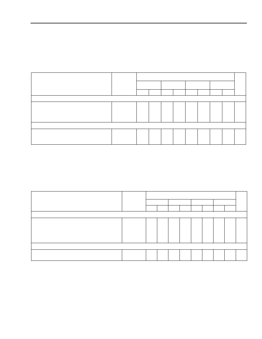
Table 46. PFU Output MUX and Direct Routing Timing Characteristics
OR3Cxx Commercial: VDD = 5.0 V ± 5%, 0 °C
< TA < 70 °C; Industrial: VDD = 5.0 V ± 10%, –40 °C < TA < +85 °C.
OR3Txxx Commercial: VDD = 3.0 V to 3.6 V, 0 °C
< TA < 70 °C; Industrial: VDD = 3.0 V to 3.6 V, –40 °C < TA < +85 °C.
* This is general feedback using switching segments. See the combinatorial PFU timing table for softwired look-up table feedback timing.
SLIC Timing
Table 47
. Supplemental Logic and Interconnect Cell (SLIC) Timing Characteristics
OR3Cxx Commercial: VDD = 5.0 V ± 5%, 0 °C
< TA < 70 °C; Industrial: VDD = 5.0 V ± 10%, –40 °C < TA < +85 °C.
OR3Txxx Commercial: VDD = 3.0 V to 3.6 V, 0 °C
< TA < 70 °C; Industrial: VDD = 3.0 V to 3.6 V, –40 °C < TA < +85 °C.
Parameter
(TJ = 85 °C, VDD = min)
Symbol
Speed
Unit
-4
-5
-6
-7
Min
Max
Min
Max
Min
Max
Min
Max
PFU Output MUX
(Fan-out = 1)
Output MUX Delay (F[7:0]/Q[7:0] to O[9:0])
Carry-out MUX Delay (COUT to O9)
Registered Carry-out MUX Delay (REGCOUT
to O8)
OMUX_DEL
COO9_DEL
RCOO8_DEL
—
0.50
0.34
—
0.39
0.26
—
0.35
0.24
—
0.28
0.18
ns
Direct Routing
PFU Feedback (xSW)*
PFU to Orthogonal PFU Delay (xSW to xSW)
PFU to Diagonal PFU Delay (xBID to xSW)
FDBK_DEL
ODIR_DEL
DDIR_DEL
—
1.74
2.21
2.69
—
1.41
1.77
2.19
—
1.48
1.75
2.53
—
1.14
1.39
1.98
ns
Parameter
(TJ = 85 °C, VDD = min)
Symbol
Speed
Unit
-4
-5
-6
-7
Min
Max
Min
Max
Min
Max
Min
Max
3-Statable BIDIs
BIDI Delay (BRx to BLx, BLx to BRx)
BIDI Delay (Ox to BRx, Ox to BLx)
BIDI 3-state Enable/Disable Delay (TRI to BL, BR)
BIDI 3-state Enable/Disable Delay
(BL, BR via DEC, TRI to BL, BR)
BUF_DEL
OBUF_DEL
TRI_DEL
DECTRI_DEL
—
0.84
0.72
2.55
3.59
—
0.70
0.61
1.90
2.65
—
0.94
0.87
1.31
1.91
—
0.77
0.70
1.01
1.48
ns
Decoder
Decoder Delay (BR[9:8], BL[9:8] to DEC)
Decoder Delay (BR[7:0], BL[7:0] to DEC)
DEC98_DEL
DEC_DEL
—
2.39
2.35
—
1.85
1.82
—
1.27
1.23
—
1.02
0.99
ns
Select
devices
have
been
discontinued.
See
Ordering
Information
section
for
product
status.
相关PDF资料 |
PDF描述 |
|---|---|
| OR3T556PS240-DB | FPGA, 324 CLBS, 80000 GATES, PQFP240 |
| OR3T806PS240-DB | FPGA, 484 CLBS, 116000 GATES, PQFP240 |
| OR3T807PS240-DB | FPGA, 484 CLBS, 116000 GATES, PQFP240 |
| OR3T55-4BA256I | FPGA, 324 CLBS, 40000 GATES, 80 MHz, PBGA256 |
| OR3T55-4BA256 | FPGA, 324 CLBS, 40000 GATES, 80 MHz, PBGA256 |
相关代理商/技术参数 |
参数描述 |
|---|---|
| OR3T30-7S240I | 制造商:未知厂家 制造商全称:未知厂家 功能描述:Field Programmable Gate Array (FPGA) |
| OR3T55 | 制造商:AGERE 制造商全称:AGERE 功能描述:3C and 3T Field-Programmable Gate Arrays |
| OR3T55-4BA256I | 制造商:未知厂家 制造商全称:未知厂家 功能描述:Field Programmable Gate Array (FPGA) |
| OR3T55-4PS208I | 制造商:未知厂家 制造商全称:未知厂家 功能描述:Field Programmable Gate Array (FPGA) |
| OR3T55-4PS240I | 制造商:未知厂家 制造商全称:未知厂家 功能描述:Field Programmable Gate Array (FPGA) |
发布紧急采购,3分钟左右您将得到回复。