- 您现在的位置:买卖IC网 > PDF目录299575 > OR3T307S240-DB (LATTICE SEMICONDUCTOR CORP) FPGA, 196 CLBS, 48000 GATES, PQFP240 PDF资料下载
参数资料
| 型号: | OR3T307S240-DB |
| 厂商: | LATTICE SEMICONDUCTOR CORP |
| 元件分类: | FPGA |
| 英文描述: | FPGA, 196 CLBS, 48000 GATES, PQFP240 |
| 封装: | PLASTIC, SQFP-240 |
| 文件页数: | 5/203页 |
| 文件大小: | 1368K |
| 代理商: | OR3T307S240-DB |
第1页第2页第3页第4页当前第5页第6页第7页第8页第9页第10页第11页第12页第13页第14页第15页第16页第17页第18页第19页第20页第21页第22页第23页第24页第25页第26页第27页第28页第29页第30页第31页第32页第33页第34页第35页第36页第37页第38页第39页第40页第41页第42页第43页第44页第45页第46页第47页第48页第49页第50页第51页第52页第53页第54页第55页第56页第57页第58页第59页第60页第61页第62页第63页第64页第65页第66页第67页第68页第69页第70页第71页第72页第73页第74页第75页第76页第77页第78页第79页第80页第81页第82页第83页第84页第85页第86页第87页第88页第89页第90页第91页第92页第93页第94页第95页第96页第97页第98页第99页第100页第101页第102页第103页第104页第105页第106页第107页第108页第109页第110页第111页第112页第113页第114页第115页第116页第117页第118页第119页第120页第121页第122页第123页第124页第125页第126页第127页第128页第129页第130页第131页第132页第133页第134页第135页第136页第137页第138页第139页第140页第141页第142页第143页第144页第145页第146页第147页第148页第149页第150页第151页第152页第153页第154页第155页第156页第157页第158页第159页第160页第161页第162页第163页第164页第165页第166页第167页第168页第169页第170页第171页第172页第173页第174页第175页第176页第177页第178页第179页第180页第181页第182页第183页第184页第185页第186页第187页第188页第189页第190页第191页第192页第193页第194页第195页第196页第197页第198页第199页第200页第201页第202页第203页
102
Lattice Semiconductor
Data Sheet
November 2006
ORCA Series 3C and 3T FPGAs
Timing Characteristics (continued)
In addition to supply voltage, process variation, and
operating temperature, circuit and process improve-
ments of the
ORCA Series FPGAs over time will result
in signicant improvement of the actual performance
over those listed for a speed grade. Even though lower
speed grades may still be available, the distribution of
yield to timing parameters may be several speed
grades higher than that designated on a product brand.
Design practices need to consider best-case timing
parameters (e.g., delays = 0), as well as worst-case
timing.
The routing delays are a function of fan-out and the
capacitance associated with the CIPs and metal inter-
connect in the path. The number of logic elements that
can be driven (fan-out) by PFUs is unlimited, although
the delay to reach a valid logic level can exceed timing
requirements. It is difcult to make accurate routing
delay estimates prior to design compilation based on
fan-out. This is because the CAE software may delete
redundant logic inserted by the designer to reduce fan-
out, and/or it may also automatically reduce fan-out by
net splitting.
The waveform test points are given in the Input/Output
Buffer Measurement Conditions section of this data
sheet. The timing parameters given in the electrical
characteristics tables in this data sheet follow industry
practices, and the values they reect are described
below.
Propagation Delay—The time between the specied
reference points. The delays provided are the worst
case of the tphh and tpll delays for noninverting func-
tions, tplh and tphl for inverting functions, and tphz and
tplz for 3-state enable.
Setup Time—The interval immediately preceding the
transition of a clock or latch enable signal, during which
the data must be stable to ensure it is recognized as
the intended value.
Hold Time—The interval immediately following the
transition of a clock or latch enable signal, during which
the data must be held stable to ensure it is recognized
as the intended value.
3-State Enable—The time from when a 3-state control
signal becomes active and the output pad reaches the
high-impedance state.
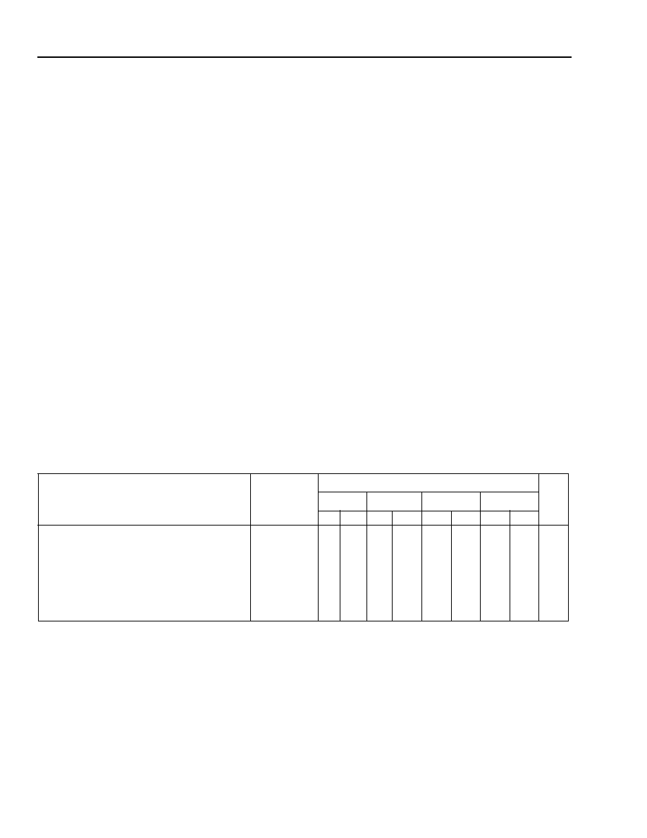
PFU Timing
* Four-input variables’ (KZ[3:0]) path delays are valid for LUTs in both F4 (four-input LUT) and F5 (ve-input LUT) modes.
Table 41. Combinatorial PFU Timing Characteristics
OR3Cxx Commercial: VDD = 5.0 V ± 5%, 0 °C
< TA < 70 °C; Industrial: VDD = 5.0 V ± 10%, –40 °C < TA < +85 °C.
OR3Txxx Commercial: VDD = 3.0 V to 3.6 V, 0 °C
< TA < 70 °C; Industrial: VDD = 3.0 V to 3.6 V, –40 °C < TA < +85 °C.
Parameter
Symbol
Speed
Unit
-4
-5
-6
-7
Min Max
Min
Max
Min
Max
Min
Max
Combinatorial Delays (TJ = +85 °C, VDD = min):
Four-input Variables (Kz[3:0] to F[z])*
Five-input Variables (F5[A:D] to F[0, 2, 4, 6])
Two-level LUT Delay (Kz[3:0] to F w/feedbk)*
Two-level LUT Delay (F5[A:D] to F w/feedbk)
Three-level LUT Delay (Kz[3:0] to F w/feedbk)*
Three-level LUT Delay (F5[A:D] to F w/feedbk)
CIN to COUT Delay (logic mode)
F4_DEL
F5_DEL
SWL2_DEL
SWL2F5_DEL
SWL3_DEL
SWL3F5_DEL
CO_DEL
—
2.34
2.11
4.87
4.69
6.93
6.89
3.47
—
1.80
1.57
3.66
3.51
5.15
5.08
2.65
—
1.32
1.23
2.58
2.48
3.63
3.54
1.79
—
1.05
0.99
2.03
1.94
2.82
2.75
1.43
ns
Select
devices
have
been
discontinued.
See
Ordering
Information
section
for
product
status.
相关PDF资料 |
PDF描述 |
|---|---|
| OR3T556PS240-DB | FPGA, 324 CLBS, 80000 GATES, PQFP240 |
| OR3T806PS240-DB | FPGA, 484 CLBS, 116000 GATES, PQFP240 |
| OR3T807PS240-DB | FPGA, 484 CLBS, 116000 GATES, PQFP240 |
| OR3T55-4BA256I | FPGA, 324 CLBS, 40000 GATES, 80 MHz, PBGA256 |
| OR3T55-4BA256 | FPGA, 324 CLBS, 40000 GATES, 80 MHz, PBGA256 |
相关代理商/技术参数 |
参数描述 |
|---|---|
| OR3T30-7S240I | 制造商:未知厂家 制造商全称:未知厂家 功能描述:Field Programmable Gate Array (FPGA) |
| OR3T55 | 制造商:AGERE 制造商全称:AGERE 功能描述:3C and 3T Field-Programmable Gate Arrays |
| OR3T55-4BA256I | 制造商:未知厂家 制造商全称:未知厂家 功能描述:Field Programmable Gate Array (FPGA) |
| OR3T55-4PS208I | 制造商:未知厂家 制造商全称:未知厂家 功能描述:Field Programmable Gate Array (FPGA) |
| OR3T55-4PS240I | 制造商:未知厂家 制造商全称:未知厂家 功能描述:Field Programmable Gate Array (FPGA) |
发布紧急采购,3分钟左右您将得到回复。