- 您现在的位置:买卖IC网 > PDF目录299575 > OR3T307S240-DB (LATTICE SEMICONDUCTOR CORP) FPGA, 196 CLBS, 48000 GATES, PQFP240 PDF资料下载
参数资料
| 型号: | OR3T307S240-DB |
| 厂商: | LATTICE SEMICONDUCTOR CORP |
| 元件分类: | FPGA |
| 英文描述: | FPGA, 196 CLBS, 48000 GATES, PQFP240 |
| 封装: | PLASTIC, SQFP-240 |
| 文件页数: | 196/203页 |
| 文件大小: | 1368K |
| 代理商: | OR3T307S240-DB |
第1页第2页第3页第4页第5页第6页第7页第8页第9页第10页第11页第12页第13页第14页第15页第16页第17页第18页第19页第20页第21页第22页第23页第24页第25页第26页第27页第28页第29页第30页第31页第32页第33页第34页第35页第36页第37页第38页第39页第40页第41页第42页第43页第44页第45页第46页第47页第48页第49页第50页第51页第52页第53页第54页第55页第56页第57页第58页第59页第60页第61页第62页第63页第64页第65页第66页第67页第68页第69页第70页第71页第72页第73页第74页第75页第76页第77页第78页第79页第80页第81页第82页第83页第84页第85页第86页第87页第88页第89页第90页第91页第92页第93页第94页第95页第96页第97页第98页第99页第100页第101页第102页第103页第104页第105页第106页第107页第108页第109页第110页第111页第112页第113页第114页第115页第116页第117页第118页第119页第120页第121页第122页第123页第124页第125页第126页第127页第128页第129页第130页第131页第132页第133页第134页第135页第136页第137页第138页第139页第140页第141页第142页第143页第144页第145页第146页第147页第148页第149页第150页第151页第152页第153页第154页第155页第156页第157页第158页第159页第160页第161页第162页第163页第164页第165页第166页第167页第168页第169页第170页第171页第172页第173页第174页第175页第176页第177页第178页第179页第180页第181页第182页第183页第184页第185页第186页第187页第188页第189页第190页第191页第192页第193页第194页第195页当前第196页第197页第198页第199页第200页第201页第202页第203页
92
Lattice Semiconductor
Data Sheet
November 2006
ORCA Series 3C and 3T FPGAs
FPGA Conguration Modes (continued)
Asynchronous Peripheral Mode
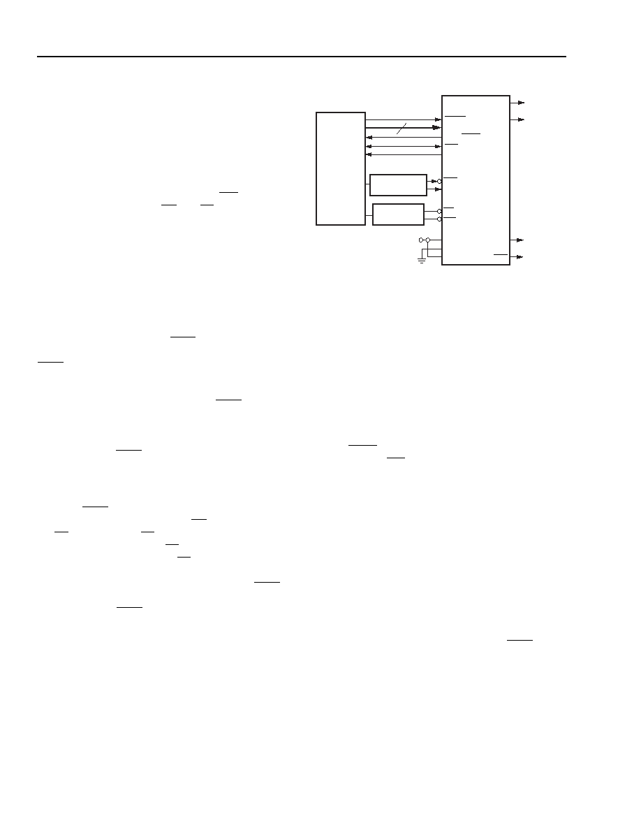
Figure 56 shows the connections needed for the asyn-
chronous peripheral mode. In this mode, the FPGA
system interface is similar to that of a microprocessor-
peripheral interface. The microprocessor generates the
control signals to write an 8-bit byte into the FPGA. The
FPGA control inputs include active-low CS0 and active-
high CS1 chip selects and WR and RD inputs. The chip
selects can be cycled or maintained at a static level
during the conguration cycle. Each byte of data is writ-
ten into the FPGA’s D[7:0] input pins. D[7:0] of the
FPGA can be connected to D[7:0] of the microproces-
sor only if a standard prom le format is used. If a .bit
or .rbt le is used from ispLEVER, then the user must
mirror the bytes in the .bit or .rbt le OR leave the .bit or
.rbt le unchanged and connect D[7:0] of the FPGA to
D[0:7] of the microprocessor.
The FPGA provides an RDY/BUSY status output to indi-
cate that another byte can be loaded. A low on RDY/
BUSY
indicates that the double-buffered hold/shift reg-
isters are not ready to receive data, and this pin must
be monitored to go high before another byte of data
can be written. The shortest time RDY/BUSY is low
occurs when a byte is loaded into the hold register and
the shift register is empty, in which case the byte is
immediately transferred to the shift register. The long-
est time for RDY/BUSY to remain low occurs when a
byte is loaded into the holding register and the shift
register has just started shifting conguration data into
conguration RAM.
The RDY/BUSY status is also available on the D7 pin by
enabling the chip selects, setting WR high, and apply-
ing RD low, where the RD input provides an output
enable for the D7 pin when RD is low. The D[6:0] pins
are not enabled to drive when RD is low and, therefore,
only act as input pins in asynchronous peripheral
mode. Optionally, the user can ignore the RDY/BUSY
status and simply wait until the maximum time it would
take for the RDY/BUSY line to go high, indicating the
FPGA is ready for more data, before writing the next
data byte.
Figure 56. Asynchronous Peripheral Conguration
Microprocessor Interface
(MPI) Mode
The built-in MPI in Series 3 FPGAs is designed for use
in conguring the FPGA. Figure 57 and Figure 58 show
the glueless interface for FPGA conguration and read-
back from the
PowerPC and i960 processors, respec-
tively. When enabled by the mode pins, the MPI
handles all conguration/readback control and hand-
shaking with the host processor. For single FPGA con-
guration, the host sets the conguration control
register PRGM bit to zero then back to a one and, after
reading that the INIT signal is high in the MPI status
register, transfers data 8 bits at a time to the FPGA’s
D[7:0] input pins.
If conguring multiple FPGAs through daisy-chain
operation is desired, the MP_DAISY bit must be set in
the conguration control register of the MPI. Because
of the latency involved in a daisy-chain conguration,
the MP_HOLD_BUS bit may be set to zero rather than
one for daisy-chain operation. This allows the MPI to
acknowledge the data transfer before the conguration
information has been serialized and transferred on the
FPGA daisy-chain. The early acknowledgment frees
the host processor to perform other system tasks. Con-
guring with the MP_HOLD_BUS bit at zero requires
that the host microprocessor poll the RDY/BUSY bit of
the MPI status register and/or use the MPI interrupt
capability to conrm the readiness of the MPI for more
conguration data.
MICRO-
PROCESSOR
D[7:0]
CS1
M2
M1
M0
HDC
ORCA
SERIES
FPGA
8
LDC
VDD
DONE
CS0
DOUT
CCLK
TO DAISY-
CHAINED
DEVICES
BUS
CONTROLLER
ADDRESS
DECODE LOGIC
RD
WR
RDY/BUSY
INIT
PRGM
Select
devices
have
been
discontinued.
See
Ordering
Information
section
for
product
status.
相关PDF资料 |
PDF描述 |
|---|---|
| OR3T556PS240-DB | FPGA, 324 CLBS, 80000 GATES, PQFP240 |
| OR3T806PS240-DB | FPGA, 484 CLBS, 116000 GATES, PQFP240 |
| OR3T807PS240-DB | FPGA, 484 CLBS, 116000 GATES, PQFP240 |
| OR3T55-4BA256I | FPGA, 324 CLBS, 40000 GATES, 80 MHz, PBGA256 |
| OR3T55-4BA256 | FPGA, 324 CLBS, 40000 GATES, 80 MHz, PBGA256 |
相关代理商/技术参数 |
参数描述 |
|---|---|
| OR3T30-7S240I | 制造商:未知厂家 制造商全称:未知厂家 功能描述:Field Programmable Gate Array (FPGA) |
| OR3T55 | 制造商:AGERE 制造商全称:AGERE 功能描述:3C and 3T Field-Programmable Gate Arrays |
| OR3T55-4BA256I | 制造商:未知厂家 制造商全称:未知厂家 功能描述:Field Programmable Gate Array (FPGA) |
| OR3T55-4PS208I | 制造商:未知厂家 制造商全称:未知厂家 功能描述:Field Programmable Gate Array (FPGA) |
| OR3T55-4PS240I | 制造商:未知厂家 制造商全称:未知厂家 功能描述:Field Programmable Gate Array (FPGA) |
发布紧急采购,3分钟左右您将得到回复。