- 您现在的位置:买卖IC网 > PDF目录296800 > PEF22508E (INFINEON TECHNOLOGIES AG) DATACOM, PCM TRANSCEIVER, PBGA256 PDF资料下载
参数资料
| 型号: | PEF22508E |
| 厂商: | INFINEON TECHNOLOGIES AG |
| 元件分类: | 数字传输电路 |
| 英文描述: | DATACOM, PCM TRANSCEIVER, PBGA256 |
| 封装: | 17 X 17 MM, 1 MM PITCH, PLASTIC, LBGA-256 |
| 文件页数: | 163/193页 |
| 文件大小: | 10683K |
| 代理商: | PEF22508E |
第1页第2页第3页第4页第5页第6页第7页第8页第9页第10页第11页第12页第13页第14页第15页第16页第17页第18页第19页第20页第21页第22页第23页第24页第25页第26页第27页第28页第29页第30页第31页第32页第33页第34页第35页第36页第37页第38页第39页第40页第41页第42页第43页第44页第45页第46页第47页第48页第49页第50页第51页第52页第53页第54页第55页第56页第57页第58页第59页第60页第61页第62页第63页第64页第65页第66页第67页第68页第69页第70页第71页第72页第73页第74页第75页第76页第77页第78页第79页第80页第81页第82页第83页第84页第85页第86页第87页第88页第89页第90页第91页第92页第93页第94页第95页第96页第97页第98页第99页第100页第101页第102页第103页第104页第105页第106页第107页第108页第109页第110页第111页第112页第113页第114页第115页第116页第117页第118页第119页第120页第121页第122页第123页第124页第125页第126页第127页第128页第129页第130页第131页第132页第133页第134页第135页第136页第137页第138页第139页第140页第141页第142页第143页第144页第145页第146页第147页第148页第149页第150页第151页第152页第153页第154页第155页第156页第157页第158页第159页第160页第161页第162页当前第163页第164页第165页第166页第167页第168页第169页第170页第171页第172页第173页第174页第175页第176页第177页第178页第179页第180页第181页第182页第183页第184页第185页第186页第187页第188页第189页第190页第191页第192页第193页
Data Sheet
71
Rev. 1.0, 2005-06-02
OctalLIU
TM
PEF 22508 E
Functional Description
3.9
Transmit Path
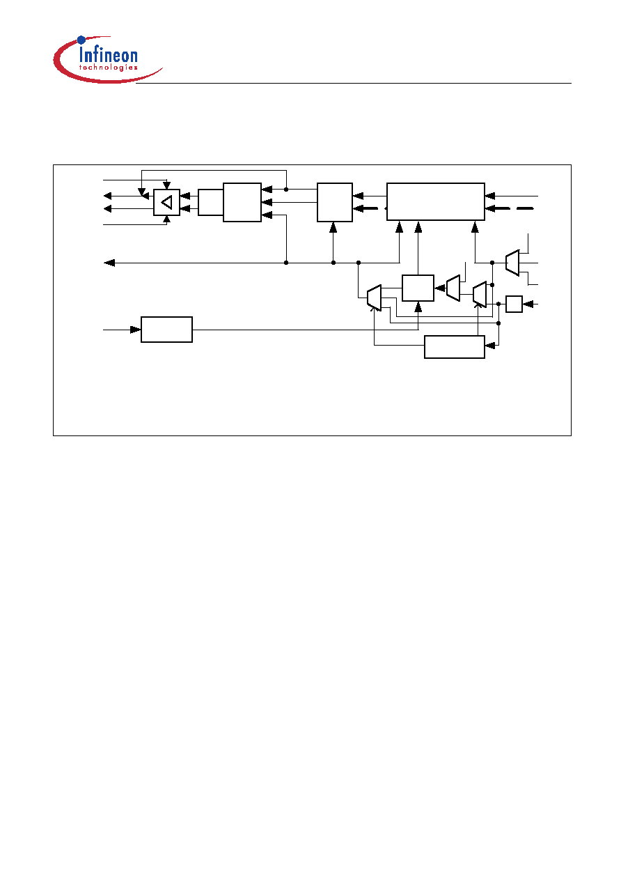
The transmit path of the OctalLIU
TM is shown in Figure 29.
Figure 29
Transmit System of one Channel
The serial transmit bit stream (single rail or dual rail) is processed by the transmitter which has the following
functions:
AIS generation (blue alarm)
Generation of In-band loop-up/-down code
3.9.1
Transmit Line Interface
The principle transmit line interface is shown in Figure 30. Two application modes are possible:
For non-generic applications pins XL3 and XL4 can be left open. The serial resistance R
SER is dependent on
the operation mode (E1/T1/J1) as shown in Table 23.
For generic E1/T1/J1 applications with optimized return loss the transmit output resistance is configured by
using the pins XL3 and XL4 as shown in Figure 30. The operation mode (E1/T1/J1) is selected by software
(register bit PC6.TSRE) without the need for external hardware changes: Here R
SER is always 2 , see
In E1 mode the value of R
Shorts between XL1 and XL2 cannot be detected, see Chapter 3.9.7.
The analog transmitter transforms the unipolar bit stream to ternary (alternate bipolar) return to zero signals of the
appropriate programmable shape. The unipolar data is provided on pin XDI and the digital transmitter.
Pulse
Shaper,
LBO
Encoder
XDIP
XCLK
XL2
DCO-X
Dual Transmit Elastic Buffer
MCLK
OctalLIU_ITS10305
Transmit Line
Interface
E: controlledby CMR2.IXSC andCMR2.IRSC
F: controlledby CMR1.DXSSandautomatic transmit clock switching
G: controlledby LIM1.RL,JATT andLIM2.ELT
H: controlledby DIC1.XBS(1:0) andautomatic transmit clock switching
%: divider: controlledby CMR6.STF(2:0)
Master
Clocking Unit
DAC
XL1/XOID
G
H
E
F
%
FCLKR
TCLK
FCLKX
Automatic Transmit
Clock Switching
recovered
receive clock
internal
transmit
clock
from
DCO-R
(in)
XL4
XL3
XDIN
相关PDF资料 |
PDF描述 |
|---|---|
| PEF22554E | DATACOM, FRAMER, PBGA160 |
| PEF22554HT | DATACOM, FRAMER, PQFP144 |
| PES12-42S-N0024 | |
| PESD3V3V4UK,132 | 25 W, UNIDIRECTIONAL, 4 ELEMENT, SILICON, TVS DIODE |
| PF38F3050L0YUQ3A | SPECIALTY MEMORY CIRCUIT, PBGA88 |
相关代理商/技术参数 |
参数描述 |
|---|---|
| PEF22508EV1.1-G | 功能描述:网络控制器与处理器 IC T/E RoHS:否 制造商:Micrel 产品:Controller Area Network (CAN) 收发器数量: 数据速率: 电源电流(最大值):595 mA 最大工作温度:+ 85 C 安装风格:SMD/SMT 封装 / 箱体:PBGA-400 封装:Tray |
| PEF22508EV11G | 制造商:Rochester Electronics LLC 功能描述: 制造商:Infineon Technologies AG 功能描述: |
| PEF22508EV11GXP | 制造商:Lantiq 功能描述:LINE INTERFACE UNITS |
| PEF22508EV11GXT | 制造商:Lantiq 功能描述:LINE INTERFACE UNITS |
| PEF22509EV1.1 | 制造商:Infineon Technologies AG 功能描述:SP000205605_T/E ASIC_TY_PB |
发布紧急采购,3分钟左右您将得到回复。