参数资料
| 型号: | XCV405E-6FG676I |
| 厂商: | Xilinx Inc |
| 文件页数: | 29/118页 |
| 文件大小: | 0K |
| 描述: | IC FPGA 1.8V 676-BGA |
| 产品变化通告: | FPGA Family Discontinuation 18/Apr/2011 |
| 标准包装: | 1 |
| 系列: | Virtex®-E EM |
| LAB/CLB数: | 2400 |
| 逻辑元件/单元数: | 10800 |
| RAM 位总计: | 573440 |
| 输入/输出数: | 404 |
| 门数: | 129600 |
| 电源电压: | 1.71 V ~ 1.89 V |
| 安装类型: | 表面贴装 |
| 工作温度: | -40°C ~ 100°C |
| 封装/外壳: | 676-BGA |
| 供应商设备封装: | 676-FBGA(27x27) |
第1页第2页第3页第4页第5页第6页第7页第8页第9页第10页第11页第12页第13页第14页第15页第16页第17页第18页第19页第20页第21页第22页第23页第24页第25页第26页第27页第28页当前第29页第30页第31页第32页第33页第34页第35页第36页第37页第38页第39页第40页第41页第42页第43页第44页第45页第46页第47页第48页第49页第50页第51页第52页第53页第54页第55页第56页第57页第58页第59页第60页第61页第62页第63页第64页第65页第66页第67页第68页第69页第70页第71页第72页第73页第74页第75页第76页第77页第78页第79页第80页第81页第82页第83页第84页第85页第86页第87页第88页第89页第90页第91页第92页第93页第94页第95页第96页第97页第98页第99页第100页第101页第102页第103页第104页第105页第106页第107页第108页第109页第110页第111页第112页第113页第114页第115页第116页第117页第118页
Virtex-E 1.8 V Extended Memory Field Programmable Gate Arrays
Module 2 of 4
DS025-2 (v3.0) March 21, 2014
14
R
— OBSOLETE — OBSOLETE — OBSOLETE — OBSOLETE —
Master-Serial Mode
In master-serial mode, the CCLK output of the FPGA drives
a Xilinx Serial PROM that feeds bit-serial data to the DIN
input. The FPGA accepts this data on each rising CCLK
edge. After the FPGA has been loaded, the data for the next
device in a daisy-chain is presented on the DOUT pin after
the rising CCLK edge.
The interface is identical to slave-serial except that an inter-
nal oscillator is used to generate the configuration clock
(CCLK). A wide range of frequencies can be selected for
CCLK which always starts at a slow default frequency. Con-
figuration bits then switch CCLK to a higher frequency for
the remainder of the configuration. Switching to a lower fre-
quency is prohibited.
The CCLK frequency is set using the ConfigRate option in
the bitstream generation software. The maximum CCLK fre-
quency that can be selected is 60 MHz. When selecting a
CCLK frequency, ensure that the serial PROM and any
daisy-chained FPGAs are fast enough to support the clock
rate.
On power-up, the CCLK frequency is approximately
2.5 MHz. This frequency is used until the ConfigRate bits
have been loaded when the frequency changes to the
selected ConfigRate. Unless a different frequency is speci-
fied in the design, the default ConfigRate is 4 MHz.
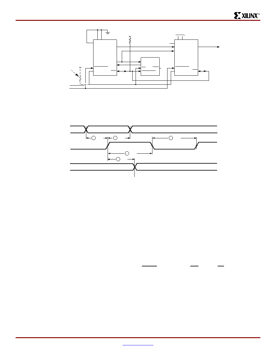
Figure 13 shows a full master/slave system. In this system,
the left-most device operates in master-serial mode. The
remaining devices operate in slave-serial mode. The SPROM
RESET pin is driven by INIT, and the CE input is driven by
DONE. There is the potential for contention on the DONE pin,
depending on the start-up sequence options chosen.
Figure 13: Master/Slave Serial Mode Circuit Diagram
VIRTEX-E
MASTER
SERIAL
VIRTEX-E,
XC4000XL,
SLAVE
XC1701L
PROGRAM
M2
M0 M1
DOUT
CCLK
CLK
3.3V
DATA
CE
CEO
RESET/OE
DONE
DIN
INIT
DONE
PROGRAM
CCLK
DIN
DOUT
M2
M0 M1
(Low Reset Option Used)
330
Ω
XCVE_ds_013_050103
N/C
Note 1: If none of the Virtex FPGAs have been selected to drive DONE, an external pull-up resistor
of 330
Ω should be added to the common DONE line. (For Spartan-XL devices, add a 4.7K Ω
pull-up resistor.) This pull-up is not needed if the DriveDONE attribute is set. If used,
DriveDONE should be selected only for the last device in the configuration chain.
Optional Pull-up
Resistor on Done
1
Figure 14: Slave-Serial Mode Programming Switching Characteristics
4 TCCH
3 TCCO
5 TCCL
2 TCCD
1 TDCC
DIN
CCLK
DOUT
(Output)
X5379_a
相关PDF资料 |
PDF描述 |
|---|---|
| BR93L86RFVM-WTR | IC EEPROM 16KBIT 2MHZ 8MSOP |
| BR93L86RFV-WE2 | IC EEPROM 16KBIT 2MHZ 8SSOP |
| BR25L020FV-WE2 | IC EEPROM SER 2KB SPI BUS 8SSOP |
| BR25L020FVM-WTR | IC EEPROM SER 2KB SPI BUS 8MSOP |
| BR25L020FVJ-WE2 | IC EEPROM 2KBIT 5MHZ 8TSSOP |
相关代理商/技术参数 |
参数描述 |
|---|---|
| XCV405E-6FG900C | 制造商:XILINX 制造商全称:XILINX 功能描述:Virtex-E 1.8 V Extended Memory Field Programmable Gate Arrays |
| XCV405E-6FG900I | 制造商:XILINX 制造商全称:XILINX 功能描述:Virtex-E 1.8 V Extended Memory Field Programmable Gate Arrays |
| XCV405E-7BG404C | 制造商:XILINX 制造商全称:XILINX 功能描述:Virtex-E 1.8 V Extended Memory Field Programmable Gate Arrays |
| XCV405E-7BG404I | 制造商:XILINX 制造商全称:XILINX 功能描述:Virtex-E 1.8 V Extended Memory Field Programmable Gate Arrays |
| XCV405E-7BG556C | 制造商:XILINX 制造商全称:XILINX 功能描述:Virtex-E 1.8 V Extended Memory Field Programmable Gate Arrays |
发布紧急采购,3分钟左右您将得到回复。