参数资料
| 型号: | XCV405E-6FG676I |
| 厂商: | Xilinx Inc |
| 文件页数: | 36/118页 |
| 文件大小: | 0K |
| 描述: | IC FPGA 1.8V 676-BGA |
| 产品变化通告: | FPGA Family Discontinuation 18/Apr/2011 |
| 标准包装: | 1 |
| 系列: | Virtex®-E EM |
| LAB/CLB数: | 2400 |
| 逻辑元件/单元数: | 10800 |
| RAM 位总计: | 573440 |
| 输入/输出数: | 404 |
| 门数: | 129600 |
| 电源电压: | 1.71 V ~ 1.89 V |
| 安装类型: | 表面贴装 |
| 工作温度: | -40°C ~ 100°C |
| 封装/外壳: | 676-BGA |
| 供应商设备封装: | 676-FBGA(27x27) |
第1页第2页第3页第4页第5页第6页第7页第8页第9页第10页第11页第12页第13页第14页第15页第16页第17页第18页第19页第20页第21页第22页第23页第24页第25页第26页第27页第28页第29页第30页第31页第32页第33页第34页第35页当前第36页第37页第38页第39页第40页第41页第42页第43页第44页第45页第46页第47页第48页第49页第50页第51页第52页第53页第54页第55页第56页第57页第58页第59页第60页第61页第62页第63页第64页第65页第66页第67页第68页第69页第70页第71页第72页第73页第74页第75页第76页第77页第78页第79页第80页第81页第82页第83页第84页第85页第86页第87页第88页第89页第90页第91页第92页第93页第94页第95页第96页第97页第98页第99页第100页第101页第102页第103页第104页第105页第106页第107页第108页第109页第110页第111页第112页第113页第114页第115页第116页第117页第118页
Virtex-E 1.8 V Extended Memory Field Programmable Gate Arrays
Module 2 of 4
DS025-2 (v3.0) March 21, 2014
20
R
— OBSOLETE — OBSOLETE — OBSOLETE — OBSOLETE —
Design Considerations
This section contains more detailed design information on
the following features.
Delay-Locked Loop . . . see page 20
BlockRAM . . . see page 24
SelectI/O . . . see page 31
Using DLLs
The Virtex-E FPGA series provides up to eight fully digital
dedicated on-chip Delay-Locked Loop (DLL) circuits which
provide zero propagation delay, low clock skew between
output clock signals distributed throughout the device, and
advanced clock domain control. These dedicated DLLs can
be used to implement several circuits which improve and
simplify system level design.
Introduction
As FPGAs grow in size, quality on-chip clock distribution
becomes increasingly important. Clock skew and clock
delay impact device performance and the task of managing
clock skew and clock delay with conventional clock trees
becomes more difficult in large devices. The Virtex-E series
of devices resolve this potential problem by providing up to
eight fully digital dedicated on-chip DLL circuits which pro-
vide zero propagation delay and low clock skew between
output clock signals distributed throughout the device.
Each DLL can drive up to two global clock routing networks
within the device. The global clock distribution network min-
imizes clock skews due to loading differences. By monitor-
ing a sample of the DLL output clock, the DLL can
compensate for the delay on the routing network, effectively
eliminating the delay from the external input port to the indi-
vidual clock loads within the device.
In addition to providing zero delay with respect to a user
source clock, the DLL can provide multiple phases of the
source clock. The DLL can also act as a clock doubler or it
can divide the user source clock by up to 16.
Clock multiplication gives the designer a number of design
alternatives. For instance, a 50 MHz source clock doubled
by the DLL can drive an FPGA design operating at 100
MHz. This technique can simplify board design because the
clock path on the board no longer distributes such a
high-speed signal. A multiplied clock also provides design-
ers the option of time-domain-multiplexing, using one circuit
twice per clock cycle, consuming less area than two copies
of the same circuit. Two DLLs in can be connected in series
to increase the effective clock multiplication factor to four.
The DLL can also act as a clock mirror. By driving the DLL
output off-chip and then back in again, the DLL can be used
to de-skew a board level clock between multiple devices.
In order to guarantee the system clock establishes prior to
the device “waking up,” the DLL can delay the completion of
the device configuration process until after the DLL
achieves lock.
By taking advantage of the DLL to remove on-chip clock
delay, the designer can greatly simplify and improve system
level design involving high-fanout, high-performance clocks.
Library DLL Symbols
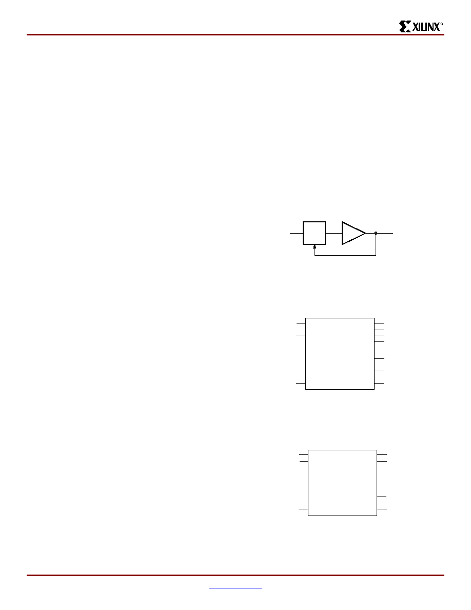
Figure 21 shows the simplified Xilinx library DLL macro
symbol, BUFGDLL. This macro delivers a quick and effi-
cient way to provide a system clock with zero propagation
the two library DLL primitives. These symbols provide
access to the complete set of DLL features when imple-
menting more complex applications.
Figure 21: Simplified DLL Macro Symbol BUFGDLL
Figure 22: Standard DLL Symbol CLKDLL
Figure 23: High Frequency DLL Symbol
0ns
ds022_25_121099
O
I
CLK0
CLK90
CLK180
CLK270
CLK2X
CLKDV
LOCKED
CLKIN
CLKFB
RST
ds022_26_121099
CLKDLL
CLK0
CLK180
CLKDV
LOCKED
CLKIN
CLKFB
RST
ds022_027_121099
CLKDLLHF
相关PDF资料 |
PDF描述 |
|---|---|
| BR93L86RFVM-WTR | IC EEPROM 16KBIT 2MHZ 8MSOP |
| BR93L86RFV-WE2 | IC EEPROM 16KBIT 2MHZ 8SSOP |
| BR25L020FV-WE2 | IC EEPROM SER 2KB SPI BUS 8SSOP |
| BR25L020FVM-WTR | IC EEPROM SER 2KB SPI BUS 8MSOP |
| BR25L020FVJ-WE2 | IC EEPROM 2KBIT 5MHZ 8TSSOP |
相关代理商/技术参数 |
参数描述 |
|---|---|
| XCV405E-6FG900C | 制造商:XILINX 制造商全称:XILINX 功能描述:Virtex-E 1.8 V Extended Memory Field Programmable Gate Arrays |
| XCV405E-6FG900I | 制造商:XILINX 制造商全称:XILINX 功能描述:Virtex-E 1.8 V Extended Memory Field Programmable Gate Arrays |
| XCV405E-7BG404C | 制造商:XILINX 制造商全称:XILINX 功能描述:Virtex-E 1.8 V Extended Memory Field Programmable Gate Arrays |
| XCV405E-7BG404I | 制造商:XILINX 制造商全称:XILINX 功能描述:Virtex-E 1.8 V Extended Memory Field Programmable Gate Arrays |
| XCV405E-7BG556C | 制造商:XILINX 制造商全称:XILINX 功能描述:Virtex-E 1.8 V Extended Memory Field Programmable Gate Arrays |
发布紧急采购,3分钟左右您将得到回复。