参数资料
| 型号: | XCV405E-6FG676I |
| 厂商: | Xilinx Inc |
| 文件页数: | 32/118页 |
| 文件大小: | 0K |
| 描述: | IC FPGA 1.8V 676-BGA |
| 产品变化通告: | FPGA Family Discontinuation 18/Apr/2011 |
| 标准包装: | 1 |
| 系列: | Virtex®-E EM |
| LAB/CLB数: | 2400 |
| 逻辑元件/单元数: | 10800 |
| RAM 位总计: | 573440 |
| 输入/输出数: | 404 |
| 门数: | 129600 |
| 电源电压: | 1.71 V ~ 1.89 V |
| 安装类型: | 表面贴装 |
| 工作温度: | -40°C ~ 100°C |
| 封装/外壳: | 676-BGA |
| 供应商设备封装: | 676-FBGA(27x27) |
第1页第2页第3页第4页第5页第6页第7页第8页第9页第10页第11页第12页第13页第14页第15页第16页第17页第18页第19页第20页第21页第22页第23页第24页第25页第26页第27页第28页第29页第30页第31页当前第32页第33页第34页第35页第36页第37页第38页第39页第40页第41页第42页第43页第44页第45页第46页第47页第48页第49页第50页第51页第52页第53页第54页第55页第56页第57页第58页第59页第60页第61页第62页第63页第64页第65页第66页第67页第68页第69页第70页第71页第72页第73页第74页第75页第76页第77页第78页第79页第80页第81页第82页第83页第84页第85页第86页第87页第88页第89页第90页第91页第92页第93页第94页第95页第96页第97页第98页第99页第100页第101页第102页第103页第104页第105页第106页第107页第108页第109页第110页第111页第112页第113页第114页第115页第116页第117页第118页
Virtex-E 1.8 V Extended Memory Field Programmable Gate Arrays
Module 2 of 4
DS025-2 (v3.0) March 21, 2014
16
R
— OBSOLETE — OBSOLETE — OBSOLETE — OBSOLETE —
either asserted or de-asserted. Otherwise an abort is
initiated, as described below.
2.
Drive data onto D[7:0]. Note that to avoid contention,
the data source should not be enabled while CS is Low
and WRITE is High. Similarly, while WRITE is High, no
more that one CS should be asserted.
3.
At the rising edge of CCLK: If BUSY is Low, the data is
accepted on this clock. If BUSY is High (from a previous
write), the data is not accepted. Acceptance instead
occurs on the first clock after BUSY goes Low, and the
data must be held until this has happened.
4.
Repeat steps 2 and 3 until all the data has been sent.
5.
De-assert CS and WRITE.
A flowchart for the write operation appears in Figure 18.
Note that if CCLK is slower than fCCNH, the FPGA never
asserts BUSY, In this case, the above handshake is unnec-
essary, and data can simply be entered into the FPGA every
CCLK cycle.
Abort
During a given assertion of CS, the user cannot switch from
a write to a read, or vice-versa. This action causes the cur-
rent packet command to be aborted. The device remains
BUSY until the aborted operation has completed. Following
an abort, data is assumed to be unaligned to word boundar-
ies, and the FPGA requires a new synchronization word
prior to accepting any new packets.
To initiate an abort during a write operation, de-assert
WRITE. At the rising edge of CCLK, an abort is initiated, as
shown in Figure 19.
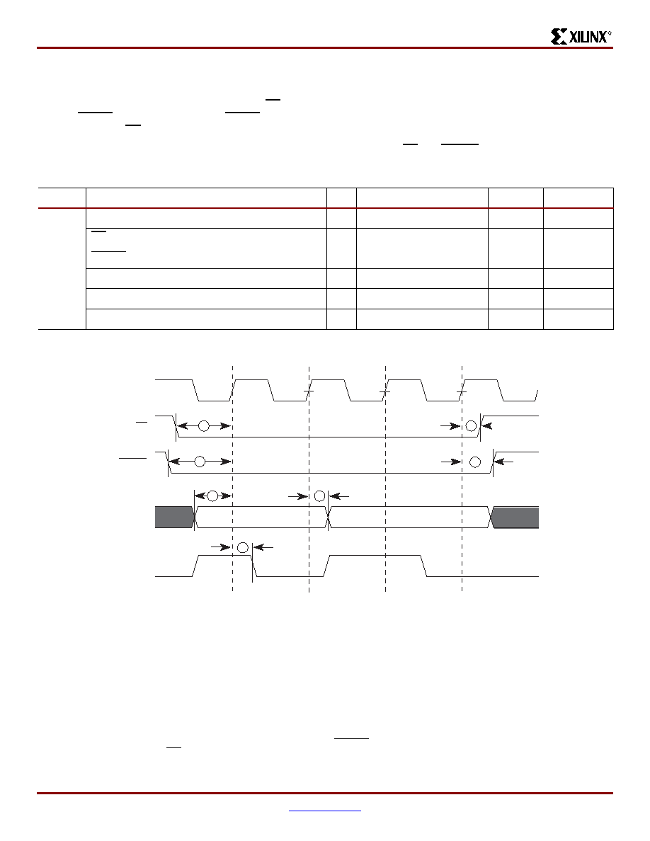
Table 11:
SelectMAP Write Timing Characteristics
Description
Symbol
Values
Units
CCLK
D0-7 Setup/Hold
1/2
TSMDCC/TSMCCD
5.0 / 1.7
ns, min
CS Setup/Hold
3/4
TSMCSCC/TSMCCCS
7.0 / 1.7
ns, min
WRITE Setup/Hold
5/6
TSMCCW/TSMWCC
7.0 / 1.7
ns, min
BUSY Propagation Delay
7
TSMCKBY
12.0
ns, max
Maximum Frequency
FCC
66
MHz, max
Maximum Frequency with no handshake
FCCNH
50
MHz, max
Figure 17: Write Operations
DS022_45_071702
CCLK
No Write
Write
No Write
Write
DATA[0:7]
CS
WRITE
3
5
BUSY
4
6
7
1
2
相关PDF资料 |
PDF描述 |
|---|---|
| BR93L86RFVM-WTR | IC EEPROM 16KBIT 2MHZ 8MSOP |
| BR93L86RFV-WE2 | IC EEPROM 16KBIT 2MHZ 8SSOP |
| BR25L020FV-WE2 | IC EEPROM SER 2KB SPI BUS 8SSOP |
| BR25L020FVM-WTR | IC EEPROM SER 2KB SPI BUS 8MSOP |
| BR25L020FVJ-WE2 | IC EEPROM 2KBIT 5MHZ 8TSSOP |
相关代理商/技术参数 |
参数描述 |
|---|---|
| XCV405E-6FG900C | 制造商:XILINX 制造商全称:XILINX 功能描述:Virtex-E 1.8 V Extended Memory Field Programmable Gate Arrays |
| XCV405E-6FG900I | 制造商:XILINX 制造商全称:XILINX 功能描述:Virtex-E 1.8 V Extended Memory Field Programmable Gate Arrays |
| XCV405E-7BG404C | 制造商:XILINX 制造商全称:XILINX 功能描述:Virtex-E 1.8 V Extended Memory Field Programmable Gate Arrays |
| XCV405E-7BG404I | 制造商:XILINX 制造商全称:XILINX 功能描述:Virtex-E 1.8 V Extended Memory Field Programmable Gate Arrays |
| XCV405E-7BG556C | 制造商:XILINX 制造商全称:XILINX 功能描述:Virtex-E 1.8 V Extended Memory Field Programmable Gate Arrays |
发布紧急采购,3分钟左右您将得到回复。