参数资料
| 型号: | XCV405E-6FG676I |
| 厂商: | Xilinx Inc |
| 文件页数: | 55/118页 |
| 文件大小: | 0K |
| 描述: | IC FPGA 1.8V 676-BGA |
| 产品变化通告: | FPGA Family Discontinuation 18/Apr/2011 |
| 标准包装: | 1 |
| 系列: | Virtex®-E EM |
| LAB/CLB数: | 2400 |
| 逻辑元件/单元数: | 10800 |
| RAM 位总计: | 573440 |
| 输入/输出数: | 404 |
| 门数: | 129600 |
| 电源电压: | 1.71 V ~ 1.89 V |
| 安装类型: | 表面贴装 |
| 工作温度: | -40°C ~ 100°C |
| 封装/外壳: | 676-BGA |
| 供应商设备封装: | 676-FBGA(27x27) |
第1页第2页第3页第4页第5页第6页第7页第8页第9页第10页第11页第12页第13页第14页第15页第16页第17页第18页第19页第20页第21页第22页第23页第24页第25页第26页第27页第28页第29页第30页第31页第32页第33页第34页第35页第36页第37页第38页第39页第40页第41页第42页第43页第44页第45页第46页第47页第48页第49页第50页第51页第52页第53页第54页当前第55页第56页第57页第58页第59页第60页第61页第62页第63页第64页第65页第66页第67页第68页第69页第70页第71页第72页第73页第74页第75页第76页第77页第78页第79页第80页第81页第82页第83页第84页第85页第86页第87页第88页第89页第90页第91页第92页第93页第94页第95页第96页第97页第98页第99页第100页第101页第102页第103页第104页第105页第106页第107页第108页第109页第110页第111页第112页第113页第114页第115页第116页第117页第118页
Virtex-E 1.8 V Extended Memory Field Programmable Gate Arrays
DS025-2 (v3.0) March 21, 2014
Module 2 of 4
37
R
— OBSOLETE — OBSOLETE — OBSOLETE — OBSOLETE —
The following list details variations of the IOBUF symbol.
IOBUF
IOBUF_S_2
IOBUF_S_4
IOBUF_S_6
IOBUF_S_8
IOBUF_S_12
IOBUF_S_16
IOBUF_S_24
IOBUF_F_2
IOBUF_F_4
IOBUF_F_6
IOBUF_F_8
IOBUF_F_12
IOBUF_F_16
IOBUF_F_24
IOBUF_LVCMOS2
IOBUF_PCI33_3
IOBUF_PCI66_3
IOBUF_GTL
IOBUF_GTLP
IOBUF_HSTL_I
IOBUF_HSTL_III
IOBUF_HSTL_IV
IOBUF_SSTL3_I
IOBUF_SSTL3_II
IOBUF_SSTL2_I
IOBUF_SSTL2_II
IOBUF_CTT
IOBUF_AGP
IOBUF_LVCMOS18
IOBUF_LVDS
IOBUF_LVPECL
When the IOBUF symbol used supports an I/O standard
that requires a differential amplifier input, the IOBUF auto-
matically configures with a differential amplifier input buffer.
The low-voltage I/O standards with a differential amplifier
input require an external reference voltage input VREF.
The voltage reference signal is “banked” within the Virtex-E
device on a half-edge basis such that for all packages there
on page 34 for a representation of the Virtex-E I/O banks.
Within each bank approximately one of every six I/O pins is
automatically configured as a VREF input. After placing a dif-
ferential amplifier input signal within a given VREF bank, the
same external source must drive all I/O pins configured as a
VREF input.
IOBUF placement restrictions require any differential ampli-
fier input signals within a bank be of the same standard.
The Virtex-E series supports eight banks for the HQ and PQ
packages. The CS package supports four VCCO banks.
Additional restrictions on the Virtex-E SelectI/O IOBUF
placement require that within a given VCCO bank each
IOBUF must share the same output source drive voltage.
Input buffers of any type and output buffers that do not
require VCCO can be placed within the same VCCO bank.
The LOC property can specify a location for the IOBUF.
An optional delay element is associated with the input path
in each IOBUF. When the IOBUF drives an input flip-flop
within the IOB, the delay element activates by default to
ensure a zero hold-time requirement. Override this default
with the NODELAY=TRUE property.
In the case when the IOBUF does not drive an input flip-flop
within the IOB, the delay element de-activates by default to
provide higher performance. To delay the input signal, acti-
vate the delay element with the DELAY=TRUE property.
3-state output buffers and bidirectional buffers can have
either a weak pull-up resistor, a weak pull-down resistor, or
a weak “keeper” circuit. Control this feature by adding the
appropriate symbol to the output net of the IOBUF (PUL-
LUP, PULLDOWN, or KEEPER).
SelectI/O Properties
Access to some of the SelectI/O features (for example, loca-
tion constraints, input delay, output drive strength, and slew
rate) is available through properties associated with these
features.
Input Delay Properties
An optional delay element is associated with each IBUF.
When the IBUF drives a flip-flop within the IOB, the delay
element activates by default to ensure a zero hold-time
requirement. Use the NODELAY=TRUE property to over-
ride this default.
In the case when the IBUF does not drive a flip-flop within
the IOB, the delay element by default de-activates to pro-
vide higher performance. To delay the input signal, activate
the delay element with the DELAY=TRUE property.
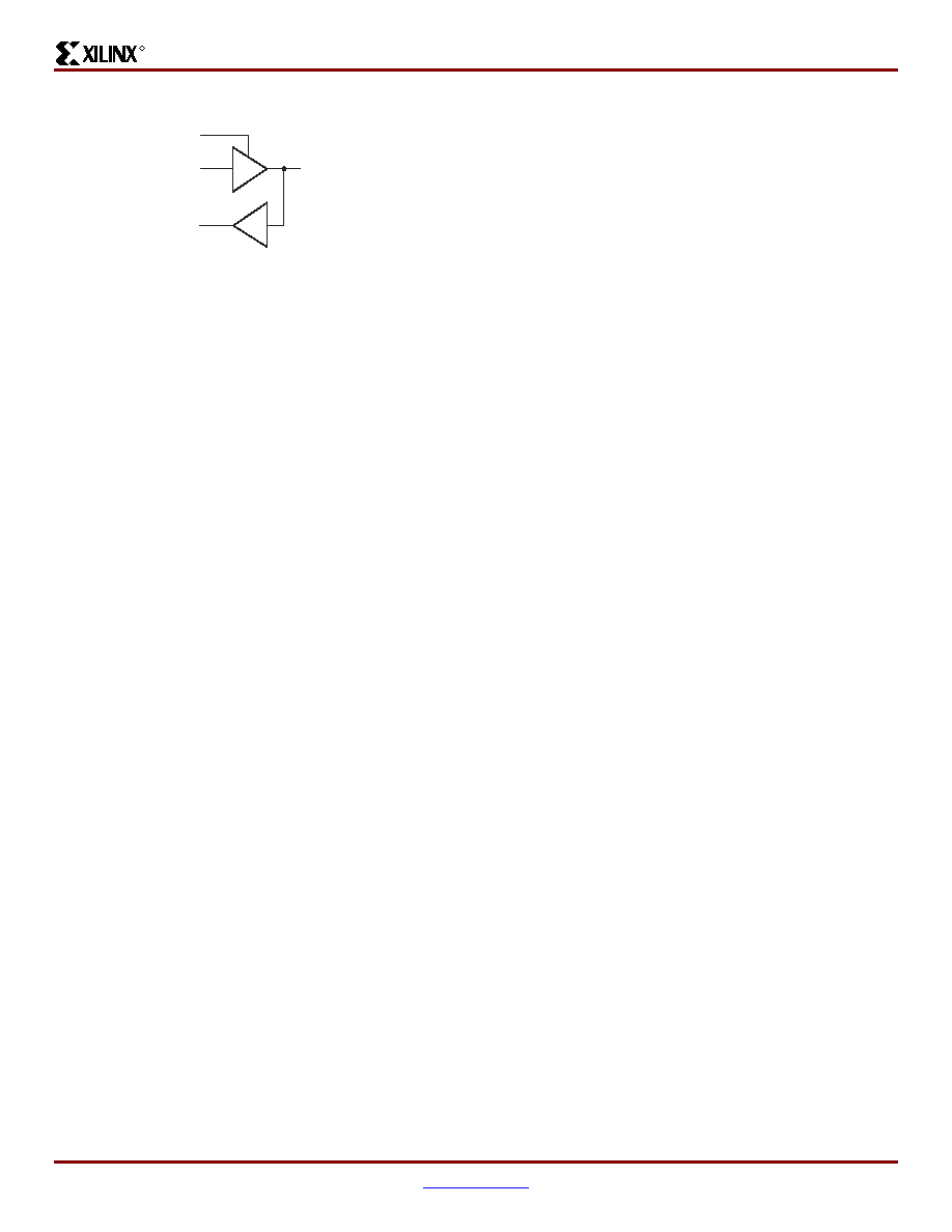
Figure 42: Input/Output Buffer Symbol (IOBUF)
IO
I
IOBUF
x133_06_111699
T
O
相关PDF资料 |
PDF描述 |
|---|---|
| BR93L86RFVM-WTR | IC EEPROM 16KBIT 2MHZ 8MSOP |
| BR93L86RFV-WE2 | IC EEPROM 16KBIT 2MHZ 8SSOP |
| BR25L020FV-WE2 | IC EEPROM SER 2KB SPI BUS 8SSOP |
| BR25L020FVM-WTR | IC EEPROM SER 2KB SPI BUS 8MSOP |
| BR25L020FVJ-WE2 | IC EEPROM 2KBIT 5MHZ 8TSSOP |
相关代理商/技术参数 |
参数描述 |
|---|---|
| XCV405E-6FG900C | 制造商:XILINX 制造商全称:XILINX 功能描述:Virtex-E 1.8 V Extended Memory Field Programmable Gate Arrays |
| XCV405E-6FG900I | 制造商:XILINX 制造商全称:XILINX 功能描述:Virtex-E 1.8 V Extended Memory Field Programmable Gate Arrays |
| XCV405E-7BG404C | 制造商:XILINX 制造商全称:XILINX 功能描述:Virtex-E 1.8 V Extended Memory Field Programmable Gate Arrays |
| XCV405E-7BG404I | 制造商:XILINX 制造商全称:XILINX 功能描述:Virtex-E 1.8 V Extended Memory Field Programmable Gate Arrays |
| XCV405E-7BG556C | 制造商:XILINX 制造商全称:XILINX 功能描述:Virtex-E 1.8 V Extended Memory Field Programmable Gate Arrays |
发布紧急采购,3分钟左右您将得到回复。