参数资料
| 型号: | XCV405E-6FG676I |
| 厂商: | Xilinx Inc |
| 文件页数: | 41/118页 |
| 文件大小: | 0K |
| 描述: | IC FPGA 1.8V 676-BGA |
| 产品变化通告: | FPGA Family Discontinuation 18/Apr/2011 |
| 标准包装: | 1 |
| 系列: | Virtex®-E EM |
| LAB/CLB数: | 2400 |
| 逻辑元件/单元数: | 10800 |
| RAM 位总计: | 573440 |
| 输入/输出数: | 404 |
| 门数: | 129600 |
| 电源电压: | 1.71 V ~ 1.89 V |
| 安装类型: | 表面贴装 |
| 工作温度: | -40°C ~ 100°C |
| 封装/外壳: | 676-BGA |
| 供应商设备封装: | 676-FBGA(27x27) |
第1页第2页第3页第4页第5页第6页第7页第8页第9页第10页第11页第12页第13页第14页第15页第16页第17页第18页第19页第20页第21页第22页第23页第24页第25页第26页第27页第28页第29页第30页第31页第32页第33页第34页第35页第36页第37页第38页第39页第40页当前第41页第42页第43页第44页第45页第46页第47页第48页第49页第50页第51页第52页第53页第54页第55页第56页第57页第58页第59页第60页第61页第62页第63页第64页第65页第66页第67页第68页第69页第70页第71页第72页第73页第74页第75页第76页第77页第78页第79页第80页第81页第82页第83页第84页第85页第86页第87页第88页第89页第90页第91页第92页第93页第94页第95页第96页第97页第98页第99页第100页第101页第102页第103页第104页第105页第106页第107页第108页第109页第110页第111页第112页第113页第114页第115页第116页第117页第118页
Virtex-E 1.8 V Extended Memory Field Programmable Gate Arrays
DS025-2 (v3.0) March 21, 2014
Module 2 of 4
25
R
— OBSOLETE — OBSOLETE — OBSOLETE — OBSOLETE —
Operating Modes
Virtex-E block SelectRAM+ memory supports two operating
modes.
Read Through
Write Back
Read Through (one clock edge)
The read address is registered on the read port clock edge
and data appears on the output after the RAM access time.
Some memories might place the latch/register at the out-
puts, depending on the desire to have a faster clock-to-out
versus set-up time. This is generally considered to be an
inferior solution, since it changes the read operation to an
asynchronous function with the possibility of missing an
address/control line transition during the generation of the read
pulse clock.
Write Back (one clock edge)
The write address is registered on the write port clock edge
and the data input is written to the memory and mirrored on
the output.
Block SelectRAM+ Characteristics
1.
All inputs are registered with the port clock and have a
set-up to clock timing specification.
2.
All outputs have a read through or write back function
depending on the state of the port WE pin. The outputs
relative to the port clock are available after the
clock-to-out timing specification.
3.
The block SelectRAM elements are true SRAM
memories and do not have a combinatorial path from
the address to the output. The LUT SelectRAM+ cells in
the CLBs are still available with this function.
4.
The ports are completely independent from each other
(i.e., clocking, control, address, read/write function, and
data width) without arbitration.
5.
A write operation requires only one clock edge.
6.
A read operation requires only one clock edge.
The output ports are latched with a self-timed circuit to guar-
antee a glitch-free read. The state of the output port does
not change until the port executes another read or write
operation.
Library Primitives
SelectRAM+ primitives. Table 14 describes all of the avail-
able primitives for synthesis and simulation.
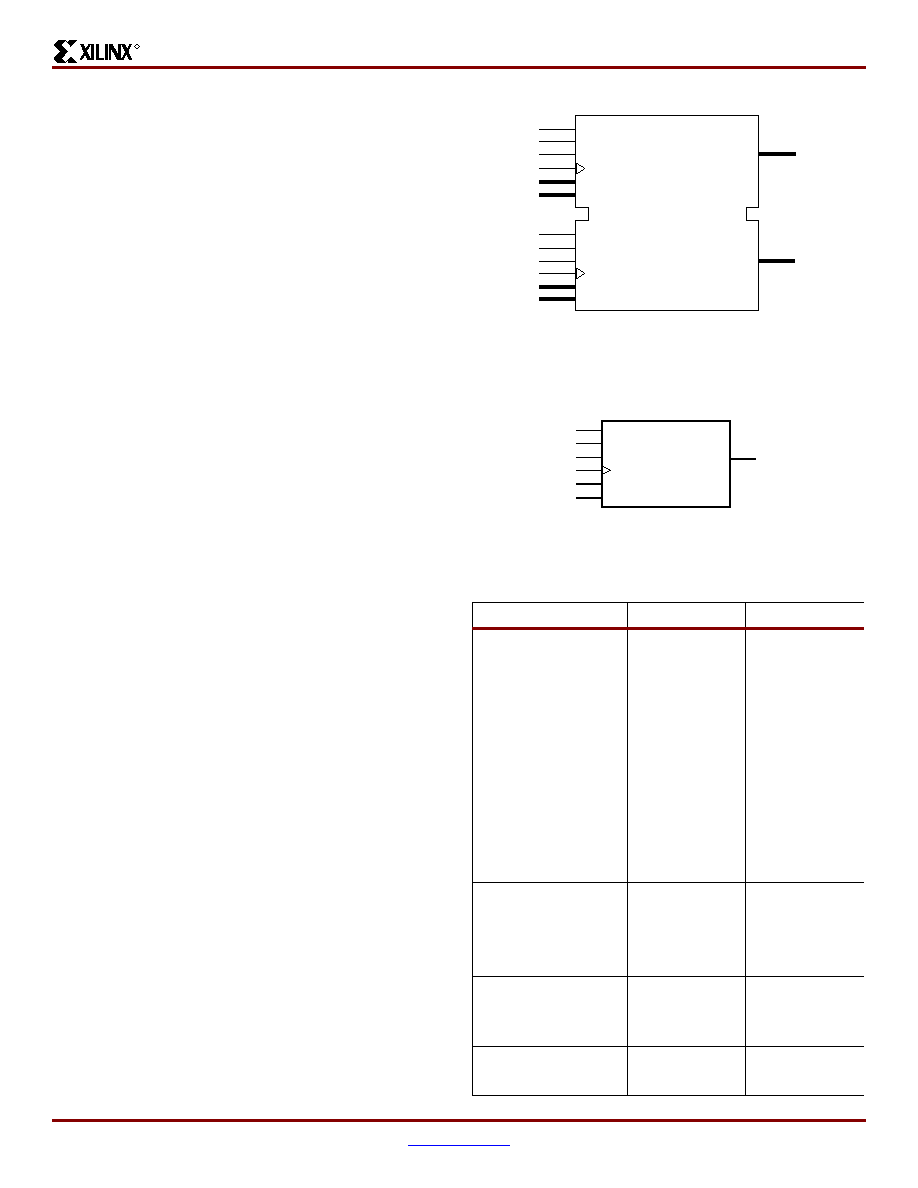
Figure 31: Dual-Port Block SelectRAM+ Memory
Figure 32: Single-Port Block SelectRAM+ Memory
Table 14:
Available Library Primitives
Primitive
Port A Width
Port B Width
RAMB4_S1
RAMB4_S1_S1
RAMB4_S1_S2
RAMB4_S1_S4
RAMB4_S1_S8
RAMB4_S1_S16
1N/A
1
2
4
8
16
RAMB4_S2
RAMB4_S2_S2
RAMB4_S2_S4
RAMB4_S2_S8
RAMB4_S2_S16
2N/A
2
4
8
16
RAMB4_S4
RAMB4_S4_S4
RAMB4_S4_S8
RAMB4_S4_S16
4N/A
4
8
16
RAMB4_S8
RAMB4_S8_S8
RAMB4_S8_S16
8N/A
8
16
RAMB4_S16
RAMB4_S16_S16
16
N/A
16
WEB
ENB
RSTB
CLKB
ADDRB[#:0]
DIB[#:0]
WEA
ENA
RSTA
CLKA
ADDRA[#:0]
DIA[#:0]
DOA[#:0]
DOB[#:0]
RAMB4_S#_S#
ds022_032_121399
ds022_033_121399
DO[#:0]
WE
EN
RST
CLK
ADDR[#:0]
DI[#:0]
RAMB4_S#
相关PDF资料 |
PDF描述 |
|---|---|
| BR93L86RFVM-WTR | IC EEPROM 16KBIT 2MHZ 8MSOP |
| BR93L86RFV-WE2 | IC EEPROM 16KBIT 2MHZ 8SSOP |
| BR25L020FV-WE2 | IC EEPROM SER 2KB SPI BUS 8SSOP |
| BR25L020FVM-WTR | IC EEPROM SER 2KB SPI BUS 8MSOP |
| BR25L020FVJ-WE2 | IC EEPROM 2KBIT 5MHZ 8TSSOP |
相关代理商/技术参数 |
参数描述 |
|---|---|
| XCV405E-6FG900C | 制造商:XILINX 制造商全称:XILINX 功能描述:Virtex-E 1.8 V Extended Memory Field Programmable Gate Arrays |
| XCV405E-6FG900I | 制造商:XILINX 制造商全称:XILINX 功能描述:Virtex-E 1.8 V Extended Memory Field Programmable Gate Arrays |
| XCV405E-7BG404C | 制造商:XILINX 制造商全称:XILINX 功能描述:Virtex-E 1.8 V Extended Memory Field Programmable Gate Arrays |
| XCV405E-7BG404I | 制造商:XILINX 制造商全称:XILINX 功能描述:Virtex-E 1.8 V Extended Memory Field Programmable Gate Arrays |
| XCV405E-7BG556C | 制造商:XILINX 制造商全称:XILINX 功能描述:Virtex-E 1.8 V Extended Memory Field Programmable Gate Arrays |
发布紧急采购,3分钟左右您将得到回复。