参数资料
| 型号: | XCV405E-6FG676I |
| 厂商: | Xilinx Inc |
| 文件页数: | 86/118页 |
| 文件大小: | 0K |
| 描述: | IC FPGA 1.8V 676-BGA |
| 产品变化通告: | FPGA Family Discontinuation 18/Apr/2011 |
| 标准包装: | 1 |
| 系列: | Virtex®-E EM |
| LAB/CLB数: | 2400 |
| 逻辑元件/单元数: | 10800 |
| RAM 位总计: | 573440 |
| 输入/输出数: | 404 |
| 门数: | 129600 |
| 电源电压: | 1.71 V ~ 1.89 V |
| 安装类型: | 表面贴装 |
| 工作温度: | -40°C ~ 100°C |
| 封装/外壳: | 676-BGA |
| 供应商设备封装: | 676-FBGA(27x27) |
第1页第2页第3页第4页第5页第6页第7页第8页第9页第10页第11页第12页第13页第14页第15页第16页第17页第18页第19页第20页第21页第22页第23页第24页第25页第26页第27页第28页第29页第30页第31页第32页第33页第34页第35页第36页第37页第38页第39页第40页第41页第42页第43页第44页第45页第46页第47页第48页第49页第50页第51页第52页第53页第54页第55页第56页第57页第58页第59页第60页第61页第62页第63页第64页第65页第66页第67页第68页第69页第70页第71页第72页第73页第74页第75页第76页第77页第78页第79页第80页第81页第82页第83页第84页第85页当前第86页第87页第88页第89页第90页第91页第92页第93页第94页第95页第96页第97页第98页第99页第100页第101页第102页第103页第104页第105页第106页第107页第108页第109页第110页第111页第112页第113页第114页第115页第116页第117页第118页
Virtex-E 1.8 V Extended Memory Field Programmable Gate Arrays
DS025-2 (v3.0) March 21, 2014
Module 2 of 4
3
R
— OBSOLETE — OBSOLETE — OBSOLETE — OBSOLETE —
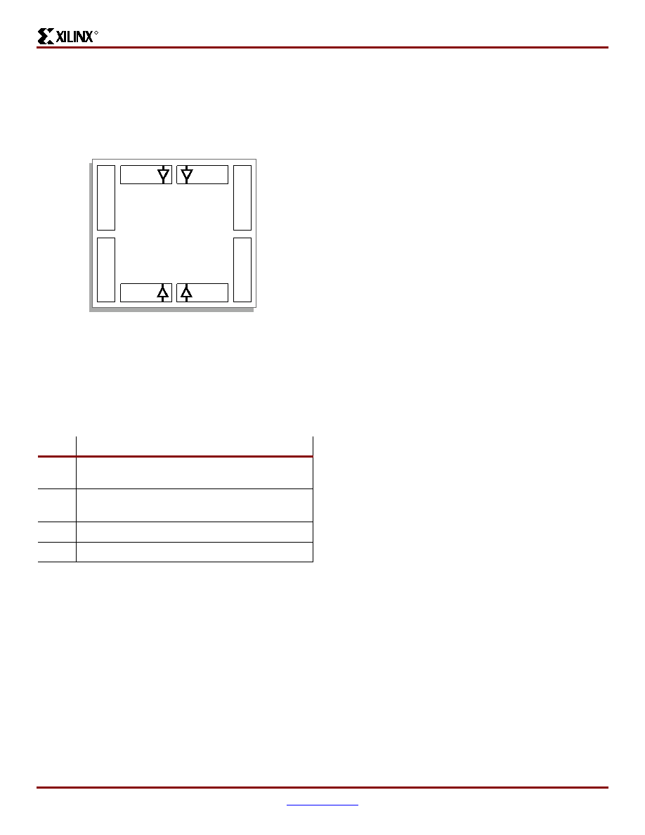
IOBs, called banks. Consequently, restrictions exist about
which I/O standards can be combined within a given bank.
Eight I/O banks result from separating each edge of the
FPGA into two banks, as shown in Figure 3. Each bank has
multiple VCCO pins, all of which must be connected to the
same voltage. This voltage is determined by the output
standards in use.
Within a bank, output standards can be mixed only if they
use the same VCCO. Compatible standards are shown in
Table 2. GTL and GTL+ appear under all voltages because
their open-drain outputs do not depend on VCCO.
Some input standards require a user-supplied threshold
voltage, VREF. In this case, certain user-I/O pins are auto-
matically configured as inputs for the VREF voltage. Approx-
imately one in six of the I/O pins in the bank assume this
role.
The VREF pins within a bank are interconnected internally
and consequently only one VREF voltage can be used within
each bank. All VREF pins in the bank, however, must be con-
nected to the external voltage source for correct operation.
Within a bank, inputs that require VREF can be mixed with
those that do not. However, only one VREF voltage can be
used within a bank.
In
Virtex-E,
input
buffers
with
LVTTL,
LVCMOS2,
LVCMOS18, PCI33_3, PCI66_3 standards are supplied by
VCCO rather than VCCINT. For these standards, only input
and output buffers that have the same VCCO can be mixed
together.
The VCCO and VREF pins for each bank appear in the device
pin-out tables and diagrams. The diagrams also show the
bank affiliation of each I/O.
Within a given package, the number of VREF and VCCO pins
can vary depending on the size of device. In larger devices,
more I/O pins convert to VREF pins. Since these are always
a super set of the VREF pins used for smaller devices, it is
possible to design a PCB that permits migration to a larger
device if necessary. All the VREF pins for the largest device
anticipated must be connected to the VREF voltage, and not
used for I/O.
In smaller devices, some VCCO pins used in larger devices
do not connect within the package. These unconnected pins
can be left unconnected externally, or they can be con-
nected to the VCCO voltage to permit migration to a larger
device, if necessary.
Configurable Logic Block
The basic building block of the Virtex-E CLB is the logic cell
(LC). An LC includes a 4-input function generator, carry
logic, and a storage element. The output from the function
generator in each LC drives both the CLB output and the D
input of the flip-flop. Each Virtex-E CLB contains four LCs,
organized in two similar slices, as shown in Figure 4.
Figure 5 shows a more detailed view of a single slice.
Figure 3: Virtex-E I/O Banks
Table 2:
Compatible Output Standards
VCCO
Compatible Standards
3.3 V
PCI, LVTTL, SSTL3 I, SSTL3 II, CTT, AGP, GTL,
GTL+, LVPECL
2.5 V
SSTL2 I, SSTL2 II, LVCMOS2, GTL, GTL+,
BLVDS, LVDS
1.8 V
LVCMOS18, GTL, GTL+
1.5 V
HSTL I, HSTL III, HSTL IV, GTL, GTL+
ds022_03_121799
Bank 0
GCLK3 GCLK2
GCLK1 GCLK0
Bank 1
Bank 5
Bank 4
VirtexE
Device
Bank
7
Bank
6
Bank
2
Bank
3
相关PDF资料 |
PDF描述 |
|---|---|
| BR93L86RFVM-WTR | IC EEPROM 16KBIT 2MHZ 8MSOP |
| BR93L86RFV-WE2 | IC EEPROM 16KBIT 2MHZ 8SSOP |
| BR25L020FV-WE2 | IC EEPROM SER 2KB SPI BUS 8SSOP |
| BR25L020FVM-WTR | IC EEPROM SER 2KB SPI BUS 8MSOP |
| BR25L020FVJ-WE2 | IC EEPROM 2KBIT 5MHZ 8TSSOP |
相关代理商/技术参数 |
参数描述 |
|---|---|
| XCV405E-6FG900C | 制造商:XILINX 制造商全称:XILINX 功能描述:Virtex-E 1.8 V Extended Memory Field Programmable Gate Arrays |
| XCV405E-6FG900I | 制造商:XILINX 制造商全称:XILINX 功能描述:Virtex-E 1.8 V Extended Memory Field Programmable Gate Arrays |
| XCV405E-7BG404C | 制造商:XILINX 制造商全称:XILINX 功能描述:Virtex-E 1.8 V Extended Memory Field Programmable Gate Arrays |
| XCV405E-7BG404I | 制造商:XILINX 制造商全称:XILINX 功能描述:Virtex-E 1.8 V Extended Memory Field Programmable Gate Arrays |
| XCV405E-7BG556C | 制造商:XILINX 制造商全称:XILINX 功能描述:Virtex-E 1.8 V Extended Memory Field Programmable Gate Arrays |
发布紧急采购,3分钟左右您将得到回复。