参数资料
| 型号: | XCV405E-6FG676I |
| 厂商: | Xilinx Inc |
| 文件页数: | 94/118页 |
| 文件大小: | 0K |
| 描述: | IC FPGA 1.8V 676-BGA |
| 产品变化通告: | FPGA Family Discontinuation 18/Apr/2011 |
| 标准包装: | 1 |
| 系列: | Virtex®-E EM |
| LAB/CLB数: | 2400 |
| 逻辑元件/单元数: | 10800 |
| RAM 位总计: | 573440 |
| 输入/输出数: | 404 |
| 门数: | 129600 |
| 电源电压: | 1.71 V ~ 1.89 V |
| 安装类型: | 表面贴装 |
| 工作温度: | -40°C ~ 100°C |
| 封装/外壳: | 676-BGA |
| 供应商设备封装: | 676-FBGA(27x27) |
第1页第2页第3页第4页第5页第6页第7页第8页第9页第10页第11页第12页第13页第14页第15页第16页第17页第18页第19页第20页第21页第22页第23页第24页第25页第26页第27页第28页第29页第30页第31页第32页第33页第34页第35页第36页第37页第38页第39页第40页第41页第42页第43页第44页第45页第46页第47页第48页第49页第50页第51页第52页第53页第54页第55页第56页第57页第58页第59页第60页第61页第62页第63页第64页第65页第66页第67页第68页第69页第70页第71页第72页第73页第74页第75页第76页第77页第78页第79页第80页第81页第82页第83页第84页第85页第86页第87页第88页第89页第90页第91页第92页第93页当前第94页第95页第96页第97页第98页第99页第100页第101页第102页第103页第104页第105页第106页第107页第108页第109页第110页第111页第112页第113页第114页第115页第116页第117页第118页
DS025-4 (v3.0) March 21, 2014
Module 4 of 4
1
2000-2014 Xilinx, Inc. All rights reserved. All Xilinx trademarks, registered trademarks, patents, and disclaimers are as listed at http://www.xilinx.com/legal.htm.
All other trademarks and registered trademarks are the property of their respective owners. All specifications are subject to change without notice.
— OBSOLETE — OBSOLETE — OBSOLETE — OBSOLETE —
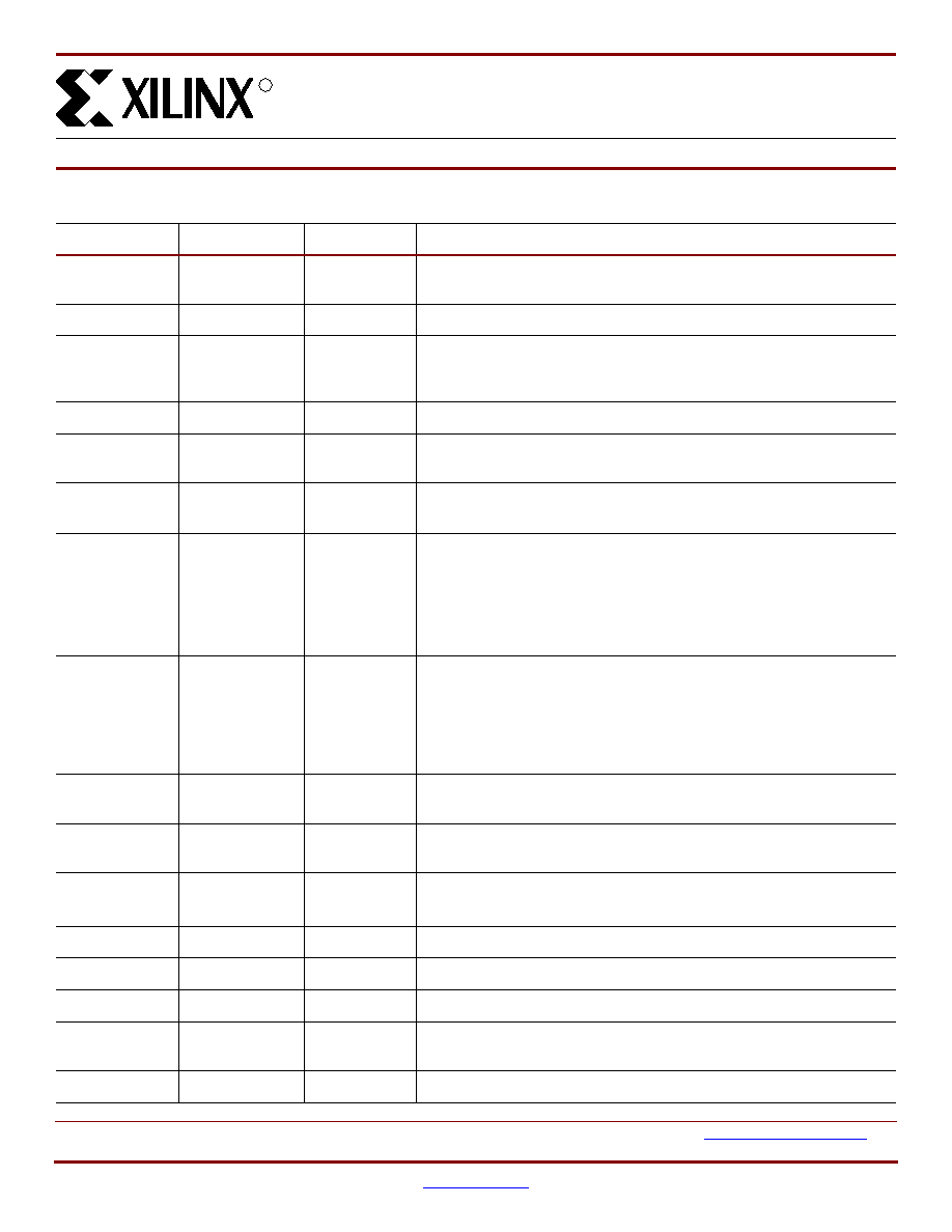
Virtex-E Pin Definitions
0
Virtex-E 1.8 V Extended Memory
Field Programmable Gate Arrays
DS025-4 (v3.0) March 21, 2014
00
Production Product Specification
R
Pin Name
Dedicated Pin
Direction
Description
GCK0, GCK1,
GCK2, GCK3
Yes
Input
Clock input pins that connect to Global Clock Buffers. These pins become
user inputs when not needed for clocks.
M0, M1, M2
Yes
Input
Mode pins are used to specify the configuration mode.
CCLK
Yes
Input or
Output
The configuration Clock I/O pin: it is an input for SelectMAP and slave-serial
modes, and output in master-serial mode. After configuration, it is input only,
logic level = Don’t Care.
PROGRAM
Yes
Input
Initiates a configuration sequence when asserted Low.
DONE
Yes
Bidirectional
Indicates that configuration loading is complete, and that the start-up
sequence is in progress. The output can be open drain.
INIT
No
Bidirectional
(Open-drain)
When Low, indicates that the configuration memory is being cleared. The pin
becomes a user I/O after configuration.
BUSY/DOUT
No
Output
In SelectMAP mode, BUSY controls the rate at which configuration data is
loaded. The pin becomes a user I/O after configuration unless the
SelectMAP port is retained.
In bit-serial modes, DOUT provides preamble and configuration data to
downstream devices in a daisy-chain. The pin becomes a user I/O after
configuration.
D0/DIN,
D1, D2,
D3, D4,
D5, D6,
D7
No
Input or
Output
In SelectMAP mode, D0-7 are configuration data pins. These pins become
user I/Os after configuration unless the SelectMAP port is retained.
In bit-serial modes, DIN is the single data input. This pin becomes a user I/O
after configuration.
WRITE
No
Input
In SelectMAP mode, the active-low Write Enable signal. The pin becomes a
user I/O after configuration unless the SelectMAP port is retained.
CS
No
Input
In SelectMAP mode, the active-low Chip Select signal. The pin becomes a
user I/O after configuration unless the SelectMAP port is retained.
TDI, TDO,
TMS, TCK
Yes
Mixed
Boundary-scan Test-Access-Port pins, as defined in IEEE1149.1.
DXN, DXP
Yes
N/A
Temperature-sensing diode pins. (Anode: DXP, cathode: DXN)
VCCINT
Yes
Input
Power-supply pins for the internal core logic.
VCCO
Yes
Input
Power-supply pins for the output drivers (subject to banking rules)
VREF
No
Input
Input threshold voltage pins. Become user I/Os when an external threshold
voltage is not needed (subject to banking rules).
GND
Yes
Input
Ground
相关PDF资料 |
PDF描述 |
|---|---|
| BR93L86RFVM-WTR | IC EEPROM 16KBIT 2MHZ 8MSOP |
| BR93L86RFV-WE2 | IC EEPROM 16KBIT 2MHZ 8SSOP |
| BR25L020FV-WE2 | IC EEPROM SER 2KB SPI BUS 8SSOP |
| BR25L020FVM-WTR | IC EEPROM SER 2KB SPI BUS 8MSOP |
| BR25L020FVJ-WE2 | IC EEPROM 2KBIT 5MHZ 8TSSOP |
相关代理商/技术参数 |
参数描述 |
|---|---|
| XCV405E-6FG900C | 制造商:XILINX 制造商全称:XILINX 功能描述:Virtex-E 1.8 V Extended Memory Field Programmable Gate Arrays |
| XCV405E-6FG900I | 制造商:XILINX 制造商全称:XILINX 功能描述:Virtex-E 1.8 V Extended Memory Field Programmable Gate Arrays |
| XCV405E-7BG404C | 制造商:XILINX 制造商全称:XILINX 功能描述:Virtex-E 1.8 V Extended Memory Field Programmable Gate Arrays |
| XCV405E-7BG404I | 制造商:XILINX 制造商全称:XILINX 功能描述:Virtex-E 1.8 V Extended Memory Field Programmable Gate Arrays |
| XCV405E-7BG556C | 制造商:XILINX 制造商全称:XILINX 功能描述:Virtex-E 1.8 V Extended Memory Field Programmable Gate Arrays |
发布紧急采购,3分钟左右您将得到回复。