参数资料
| 型号: | XCV405E-6FG676I |
| 厂商: | Xilinx Inc |
| 文件页数: | 57/118页 |
| 文件大小: | 0K |
| 描述: | IC FPGA 1.8V 676-BGA |
| 产品变化通告: | FPGA Family Discontinuation 18/Apr/2011 |
| 标准包装: | 1 |
| 系列: | Virtex®-E EM |
| LAB/CLB数: | 2400 |
| 逻辑元件/单元数: | 10800 |
| RAM 位总计: | 573440 |
| 输入/输出数: | 404 |
| 门数: | 129600 |
| 电源电压: | 1.71 V ~ 1.89 V |
| 安装类型: | 表面贴装 |
| 工作温度: | -40°C ~ 100°C |
| 封装/外壳: | 676-BGA |
| 供应商设备封装: | 676-FBGA(27x27) |
第1页第2页第3页第4页第5页第6页第7页第8页第9页第10页第11页第12页第13页第14页第15页第16页第17页第18页第19页第20页第21页第22页第23页第24页第25页第26页第27页第28页第29页第30页第31页第32页第33页第34页第35页第36页第37页第38页第39页第40页第41页第42页第43页第44页第45页第46页第47页第48页第49页第50页第51页第52页第53页第54页第55页第56页当前第57页第58页第59页第60页第61页第62页第63页第64页第65页第66页第67页第68页第69页第70页第71页第72页第73页第74页第75页第76页第77页第78页第79页第80页第81页第82页第83页第84页第85页第86页第87页第88页第89页第90页第91页第92页第93页第94页第95页第96页第97页第98页第99页第100页第101页第102页第103页第104页第105页第106页第107页第108页第109页第110页第111页第112页第113页第114页第115页第116页第117页第118页
Virtex-E 1.8 V Extended Memory Field Programmable Gate Arrays
DS025-2 (v3.0) March 21, 2014
Module 2 of 4
39
R
— OBSOLETE — OBSOLETE — OBSOLETE — OBSOLETE —
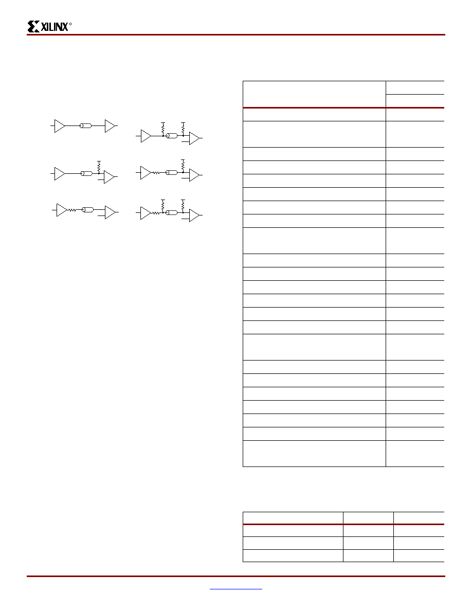
Input termination techniques include the following:
None
Parallel (Shunt)
These termination techniques can be applied in any combi-
nation. A generic example of each combination of termina-
tion methods appears in Figure 43.
Simultaneous Switching Guidelines
Ground bounce can occur with high-speed digital ICs when
multiple outputs change states simultaneously, causing
undesired transient behavior on an output, or in the internal
logic. This problem is also referred to as the Simultaneous
Switching Output (SSO) problem.
Ground bounce is primarily due to current changes in the
combined inductance of ground pins, bond wires, and
ground metallization. The IC internal ground level deviates
from the external system ground level for a short duration (a
few nanoseconds) after multiple outputs change state
simultaneously.
Ground bounce affects stable Low outputs and all inputs
because they interpret the incoming signal by comparing it
to the internal ground. If the ground bounce amplitude
exceeds the actual instantaneous noise margin, then a
non-changing input can be interpreted as a short pulse with
a polarity opposite to the ground bounce.
Table 21 provides the guidelines for the maximum number
of simultaneously switching outputs allowed per output
power/ground pair to avoid the effects of ground bounce.
Refer to Table 22 for the number of effective output
power/ground pairs for each Virtex-E device and package
combination.
Figure 43: Overview of Standard Input and Output
Termination Methods
x133_07_111699
Unterminated
Double Parallel Terminated
Series-Parallel Terminated Output
Driving a Parallel Terminated Input
V
TT
V
TT
V
REF
Series Terminated Output Driving
a Parallel Terminated Input
V
TT
V
REF
Unterminated Output Driving
a Parallel Terminated Input
V
TT
V
REF
V
TT
V
TT
V
REF
Series Terminated Output
V
REF
Z=50
Table 21:
Guidelines for Maximum Number of
Simultaneously Switching Outputs per
Power/Ground Pair
Standard
Package
BGA, FGA
LVTTL Slow Slew Rate, 2 mA drive
68
LVTTL Slow Slew Rate, 4 mA drive
41
LVTTL Slow Slew Rate, 6 mA drive
29
LVTTL Slow Slew Rate, 8 mA drive
22
LVTTL Slow Slew Rate, 12 mA drive
17
LVTTL Slow Slew Rate, 16 mA drive
14
LVTTL Slow Slew Rate, 24 mA drive
9
LVTTL Fast Slew Rate, 2 mA drive
40
LVTTL Fast Slew Rate, 4 mA drive
24
LVTTL Fast Slew Rate, 6 mA drive
17
LVTTL Fast Slew Rate, 8 mA drive
13
LVTTL Fast Slew Rate, 12 mA drive
10
LVTTL Fast Slew Rate, 16 mA drive
8
LVTTL Fast Slew Rate, 24 mA drive
5
LVCMOS
10
PCI
8
GTL
4
GTL+
4
HSTL Class I
18
HSTL Class III
9
HSTL Class IV
5
SSTL2 Class I
15
SSTL2 Class II
10
SSTL3 Class I
11
SSTL3 Class II
7
CTT
14
AGP
9
Note: This analysis assumes a 35 pF load for each output.
Table 22:
Virtex-E Extended Memory Family
Equivalent Power/Ground Pairs
Pkg/Part
XCV405E
XCV812E
BG560
56
FG676
56
FG900
相关PDF资料 |
PDF描述 |
|---|---|
| BR93L86RFVM-WTR | IC EEPROM 16KBIT 2MHZ 8MSOP |
| BR93L86RFV-WE2 | IC EEPROM 16KBIT 2MHZ 8SSOP |
| BR25L020FV-WE2 | IC EEPROM SER 2KB SPI BUS 8SSOP |
| BR25L020FVM-WTR | IC EEPROM SER 2KB SPI BUS 8MSOP |
| BR25L020FVJ-WE2 | IC EEPROM 2KBIT 5MHZ 8TSSOP |
相关代理商/技术参数 |
参数描述 |
|---|---|
| XCV405E-6FG900C | 制造商:XILINX 制造商全称:XILINX 功能描述:Virtex-E 1.8 V Extended Memory Field Programmable Gate Arrays |
| XCV405E-6FG900I | 制造商:XILINX 制造商全称:XILINX 功能描述:Virtex-E 1.8 V Extended Memory Field Programmable Gate Arrays |
| XCV405E-7BG404C | 制造商:XILINX 制造商全称:XILINX 功能描述:Virtex-E 1.8 V Extended Memory Field Programmable Gate Arrays |
| XCV405E-7BG404I | 制造商:XILINX 制造商全称:XILINX 功能描述:Virtex-E 1.8 V Extended Memory Field Programmable Gate Arrays |
| XCV405E-7BG556C | 制造商:XILINX 制造商全称:XILINX 功能描述:Virtex-E 1.8 V Extended Memory Field Programmable Gate Arrays |
发布紧急采购,3分钟左右您将得到回复。