参数资料
| 型号: | XCV405E-6FG676I |
| 厂商: | Xilinx Inc |
| 文件页数: | 34/118页 |
| 文件大小: | 0K |
| 描述: | IC FPGA 1.8V 676-BGA |
| 产品变化通告: | FPGA Family Discontinuation 18/Apr/2011 |
| 标准包装: | 1 |
| 系列: | Virtex®-E EM |
| LAB/CLB数: | 2400 |
| 逻辑元件/单元数: | 10800 |
| RAM 位总计: | 573440 |
| 输入/输出数: | 404 |
| 门数: | 129600 |
| 电源电压: | 1.71 V ~ 1.89 V |
| 安装类型: | 表面贴装 |
| 工作温度: | -40°C ~ 100°C |
| 封装/外壳: | 676-BGA |
| 供应商设备封装: | 676-FBGA(27x27) |
第1页第2页第3页第4页第5页第6页第7页第8页第9页第10页第11页第12页第13页第14页第15页第16页第17页第18页第19页第20页第21页第22页第23页第24页第25页第26页第27页第28页第29页第30页第31页第32页第33页当前第34页第35页第36页第37页第38页第39页第40页第41页第42页第43页第44页第45页第46页第47页第48页第49页第50页第51页第52页第53页第54页第55页第56页第57页第58页第59页第60页第61页第62页第63页第64页第65页第66页第67页第68页第69页第70页第71页第72页第73页第74页第75页第76页第77页第78页第79页第80页第81页第82页第83页第84页第85页第86页第87页第88页第89页第90页第91页第92页第93页第94页第95页第96页第97页第98页第99页第100页第101页第102页第103页第104页第105页第106页第107页第108页第109页第110页第111页第112页第113页第114页第115页第116页第117页第118页
Virtex-E 1.8 V Extended Memory Field Programmable Gate Arrays
Module 2 of 4
DS025-2 (v3.0) March 21, 2014
18
R
— OBSOLETE — OBSOLETE — OBSOLETE — OBSOLETE —
Configuration through the TAP uses the CFG_IN instruc-
tion. This instruction allows data input on TDI to be con-
verted into data packets for the internal configuration bus.
The following steps are required to configure the FPGA
through the boundary-scan port (when using TCK as a
start-up clock).
1.
Load the CFG_IN instruction into the boundary-scan
instruction register (IR)
2.
Enter the Shift-DR (SDR) state
3.
Shift a configuration bitstream into TDI
4.
Return to Run-Test-Idle (RTI)
5.
Load the JSTART instruction into IR
6.
Enter the SDR state
7.
Clock TCK through the startup sequence
8.
Return to RTI
Configuration and readback via the TAP is always available.
The boundary-scan mode is selected by a <101> or <001>
on the mode pins (M2, M1, M0). For details on TAP charac-
teristics, refer to XAPP139.
Configuration Sequence
The configuration of Virtex-E devices is a three-phase pro-
cess. First, the configuration memory is cleared. Next, con-
figuration data is loaded into the memory, and finally, the
logic is activated by a start-up process.
Configuration is automatically initiated on power-up unless
it is delayed by the user, as described below. The configura-
tion process can also be initiated by asserting PROGRAM.
The end of the memory-clearing phase is signalled by INIT
going High, and the completion of the entire process is sig-
nalled by DONE going High.
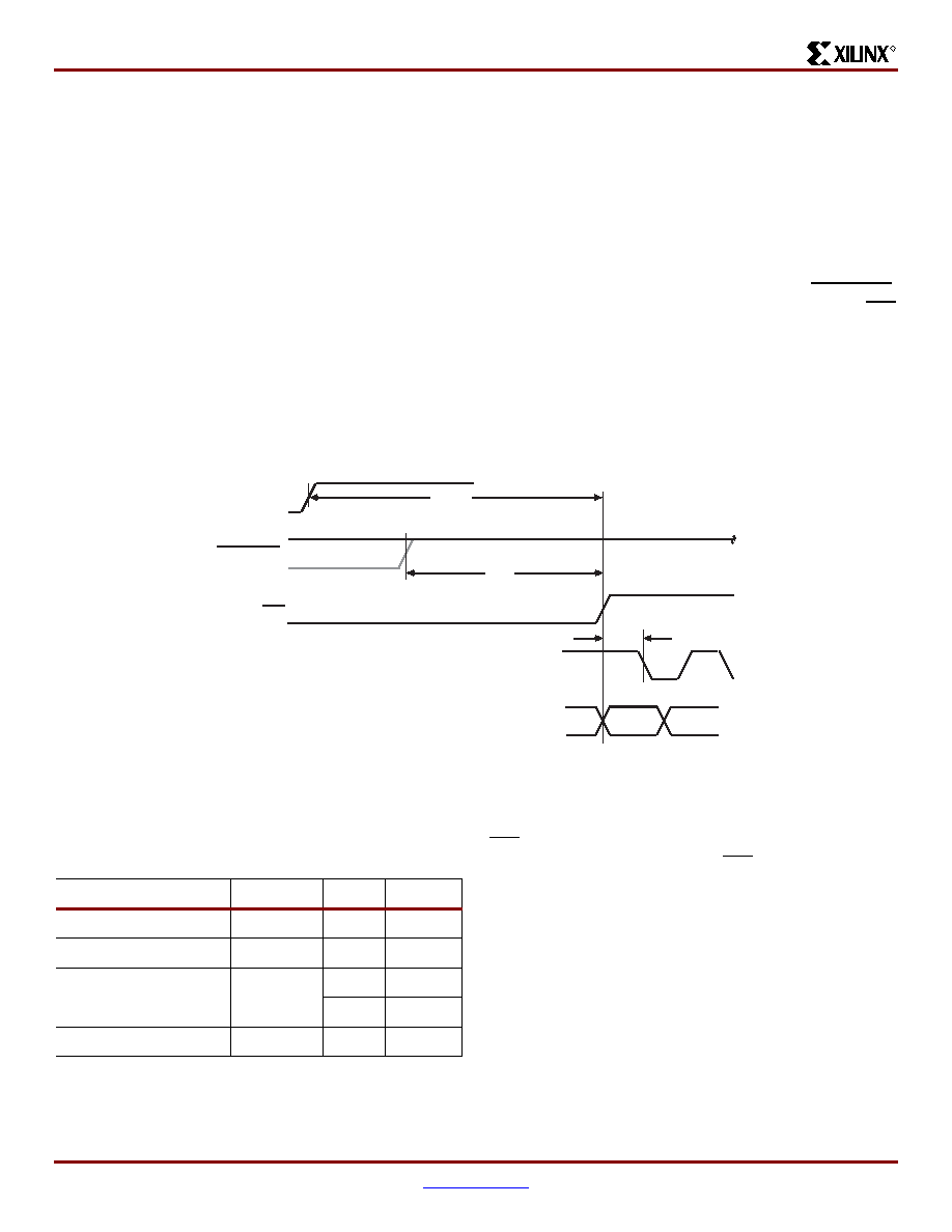
The power-up timing of configuration signals is shown in
The corresponding timing characteristics are listed in
Delaying Configuration
INIT can be held Low using an open-drain driver. An
open-drain is required since INIT is a bidirectional
open-drain pin that is held Low by the FPGA while the con-
figuration memory is being cleared. Extending the time that
the pin is Low causes the configuration sequencer to wait.
Thus, configuration is delayed by preventing entry into the
phase where data is loaded.
Start-Up Sequence
The default Start-up sequence is that one CCLK cycle after
DONE goes High, the global 3-state signal (GTS) is
released. This permits device outputs to turn on as neces-
sary.
One CCLK cycle later, the Global Set/Reset (GSR) and
Global Write Enable (GWE) signals are released. This per-
Figure 20: Power-Up Timing Configuration Signals
VALI
PROGRAM
Vcc
CCLK OUTPUT or INPUT
M0, M1, M2
(Required)
TPL
TICCK
ds022_020_071201
TPOR
INIT
Table 12:
Power-up Timing Characteristics
Description
Symbol
Value
Units
Power-on Reset1
TPOR
2.0
ms, max
Program Latency
TPL
100.0
μs, max
CCLK (output) Delay
TICCK
0.5
μs, min
4.0
μs, max
Program Pulse Width
TPROGRAM
300
ns, min
Notes:
1.
TPOR delay is the initialization time required after VCCINT
reaches the recommended operating voltage.
相关PDF资料 |
PDF描述 |
|---|---|
| BR93L86RFVM-WTR | IC EEPROM 16KBIT 2MHZ 8MSOP |
| BR93L86RFV-WE2 | IC EEPROM 16KBIT 2MHZ 8SSOP |
| BR25L020FV-WE2 | IC EEPROM SER 2KB SPI BUS 8SSOP |
| BR25L020FVM-WTR | IC EEPROM SER 2KB SPI BUS 8MSOP |
| BR25L020FVJ-WE2 | IC EEPROM 2KBIT 5MHZ 8TSSOP |
相关代理商/技术参数 |
参数描述 |
|---|---|
| XCV405E-6FG900C | 制造商:XILINX 制造商全称:XILINX 功能描述:Virtex-E 1.8 V Extended Memory Field Programmable Gate Arrays |
| XCV405E-6FG900I | 制造商:XILINX 制造商全称:XILINX 功能描述:Virtex-E 1.8 V Extended Memory Field Programmable Gate Arrays |
| XCV405E-7BG404C | 制造商:XILINX 制造商全称:XILINX 功能描述:Virtex-E 1.8 V Extended Memory Field Programmable Gate Arrays |
| XCV405E-7BG404I | 制造商:XILINX 制造商全称:XILINX 功能描述:Virtex-E 1.8 V Extended Memory Field Programmable Gate Arrays |
| XCV405E-7BG556C | 制造商:XILINX 制造商全称:XILINX 功能描述:Virtex-E 1.8 V Extended Memory Field Programmable Gate Arrays |
发布紧急采购,3分钟左右您将得到回复。