参数资料
| 型号: | XCV405E-6FG676I |
| 厂商: | Xilinx Inc |
| 文件页数: | 83/118页 |
| 文件大小: | 0K |
| 描述: | IC FPGA 1.8V 676-BGA |
| 产品变化通告: | FPGA Family Discontinuation 18/Apr/2011 |
| 标准包装: | 1 |
| 系列: | Virtex®-E EM |
| LAB/CLB数: | 2400 |
| 逻辑元件/单元数: | 10800 |
| RAM 位总计: | 573440 |
| 输入/输出数: | 404 |
| 门数: | 129600 |
| 电源电压: | 1.71 V ~ 1.89 V |
| 安装类型: | 表面贴装 |
| 工作温度: | -40°C ~ 100°C |
| 封装/外壳: | 676-BGA |
| 供应商设备封装: | 676-FBGA(27x27) |
第1页第2页第3页第4页第5页第6页第7页第8页第9页第10页第11页第12页第13页第14页第15页第16页第17页第18页第19页第20页第21页第22页第23页第24页第25页第26页第27页第28页第29页第30页第31页第32页第33页第34页第35页第36页第37页第38页第39页第40页第41页第42页第43页第44页第45页第46页第47页第48页第49页第50页第51页第52页第53页第54页第55页第56页第57页第58页第59页第60页第61页第62页第63页第64页第65页第66页第67页第68页第69页第70页第71页第72页第73页第74页第75页第76页第77页第78页第79页第80页第81页第82页当前第83页第84页第85页第86页第87页第88页第89页第90页第91页第92页第93页第94页第95页第96页第97页第98页第99页第100页第101页第102页第103页第104页第105页第106页第107页第108页第109页第110页第111页第112页第113页第114页第115页第116页第117页第118页
Virtex-E 1.8 V Extended Memory Field Programmable Gate Arrays
DS025-3 (v3.0) March 21, 2014
Module 3 of 4
11
R
— OBSOLETE — OBSOLETE — OBSOLETE — OBSOLETE —
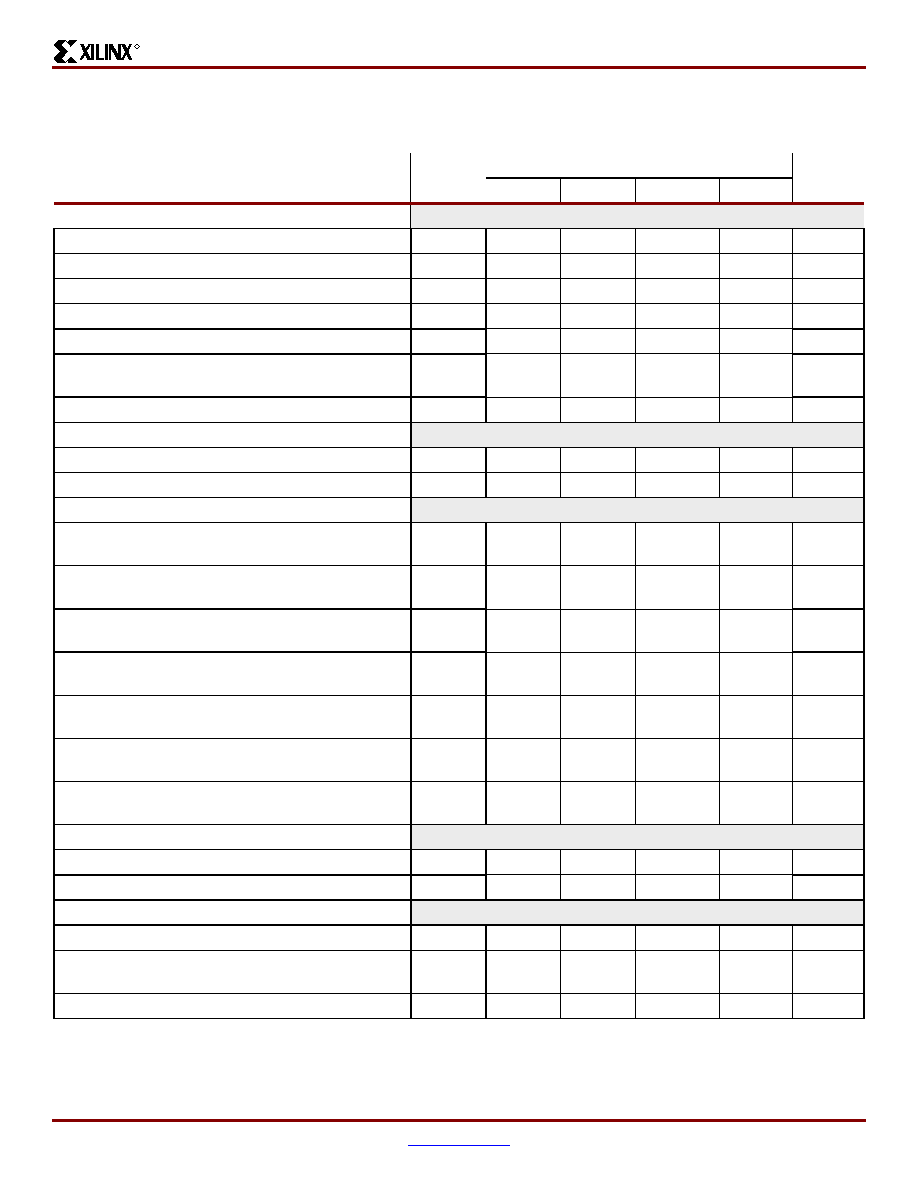
CLB Switching Characteristics
Delays originating at F/G inputs vary slightly according to the input used, see Figure 2. The values listed below are
worst-case. Precise values are provided by the timing analyzer.
Description(1)
Symbol
Speed Grade
Units
Min
-8
-7
-6
Combinatorial Delays
4-input function: F/G inputs to X/Y outputs
TILO
0.19
0.40
0.42
0.47
ns, max
5-input function: F/G inputs to F5 output
TIF5
0.36
0.76
0.8
0.9
ns, max
5-input function: F/G inputs to X output
TIF5X
0.35
0.74
0.8
0.9
ns, max
6-input function: F/G inputs to Y output via F6 MUX
TIF6Y
0.35
0.74
0.9
1.0
ns, max
6-input function: F5IN input to Y output
TF5INY
0.04
0.11
0.20
0.22
ns, max
Incremental delay routing through transparent latch
to XQ/YQ outputs
TIFNCTL
0.27
0.63
0.7
0.8
ns, max
BY input to YB output
TBYYB
0.19
0.38
0.46
0.51
ns, max
Sequential Delays
FF Clock CLK to XQ/YQ outputs
TCKO
0.34
0.78
0.9
1.0
ns, max
Latch Clock CLK to XQ/YQ outputs
TCKLO
0.40
0.77
0.9
1.0
ns, max
Setup and Hold Times before/after Clock CLK
4-input function: F/G Inputs
TICK /
TCKI
0.39 / 0
0.9 / 0
1.0 / 0
1.1 / 0
ns, min
5-input function: F/G inputs
TIF5CK /
TCKIF5
0.55 / 0
1.3 / 0
1.4 / 0
1.5 / 0
ns, min
6-input function: F5IN input
TF5INCK/
TCKF5IN
0.27 / 0
0.6 / 0
0.8 / 0
ns, min
6-input function: F/G inputs via F6 MUX
TIF6CK /
TCKIF6
0.58 / 0
1.3 / 0
1.5 / 0
1.6 / 0
ns, min
BX/BY inputs
TDICK /
TCKDI
0.25 / 0
0.6 / 0
0.7 / 0
0.8 / 0
ns, min
CE input
TCECK /
TCKCE
0.28 / 0
0.55 / 0
0.7 / 0
ns, min
SR/BY inputs (synchronous)
TRCK /
TCKR
0.24 / 0
0.46 / 0
0.52 / 0
0.6 / 0
ns, min
Clock CLK
Minimum Pulse Width, High
TCH
0.56
1.2
1.3
1.4
ns, min
Minimum Pulse Width, Low
TCL
0.56
1.2
1.3
1.4
ns, min
Set/Reset
Minimum Pulse Width, SR/BY inputs
TRPW
0.94
1.9
2.1
2.4
ns, min
Delay from SR/BY inputs to XQ/YQ outputs
(asynchronous)
TRQ
0.39
0.8
0.9
1.0
ns, max
Toggle Frequency (MHz) (for export control)
FTOG
-
416
400
357
MHz
Notes:
1.
A Zero “0” Hold Time listing indicates no hold time or a negative hold time. Negative values can not be guaranteed “best-case”, but
if a “0” is listed, there is no positive hold time.
相关PDF资料 |
PDF描述 |
|---|---|
| BR93L86RFVM-WTR | IC EEPROM 16KBIT 2MHZ 8MSOP |
| BR93L86RFV-WE2 | IC EEPROM 16KBIT 2MHZ 8SSOP |
| BR25L020FV-WE2 | IC EEPROM SER 2KB SPI BUS 8SSOP |
| BR25L020FVM-WTR | IC EEPROM SER 2KB SPI BUS 8MSOP |
| BR25L020FVJ-WE2 | IC EEPROM 2KBIT 5MHZ 8TSSOP |
相关代理商/技术参数 |
参数描述 |
|---|---|
| XCV405E-6FG900C | 制造商:XILINX 制造商全称:XILINX 功能描述:Virtex-E 1.8 V Extended Memory Field Programmable Gate Arrays |
| XCV405E-6FG900I | 制造商:XILINX 制造商全称:XILINX 功能描述:Virtex-E 1.8 V Extended Memory Field Programmable Gate Arrays |
| XCV405E-7BG404C | 制造商:XILINX 制造商全称:XILINX 功能描述:Virtex-E 1.8 V Extended Memory Field Programmable Gate Arrays |
| XCV405E-7BG404I | 制造商:XILINX 制造商全称:XILINX 功能描述:Virtex-E 1.8 V Extended Memory Field Programmable Gate Arrays |
| XCV405E-7BG556C | 制造商:XILINX 制造商全称:XILINX 功能描述:Virtex-E 1.8 V Extended Memory Field Programmable Gate Arrays |
发布紧急采购,3分钟左右您将得到回复。