- 您现在的位置:买卖IC网 > PDF目录298744 > A42MX24-3VQ100B (Electronic Theatre Controls, Inc.) 40MX and 42MX FPGA Families PDF资料下载
参数资料
| 型号: | A42MX24-3VQ100B |
| 厂商: | Electronic Theatre Controls, Inc. |
| 英文描述: | 40MX and 42MX FPGA Families |
| 中文描述: | 40MX和42MX FPGA系列 |
| 文件页数: | 21/93页 |
| 文件大小: | 854K |
| 代理商: | A42MX24-3VQ100B |
第1页第2页第3页第4页第5页第6页第7页第8页第9页第10页第11页第12页第13页第14页第15页第16页第17页第18页第19页第20页当前第21页第22页第23页第24页第25页第26页第27页第28页第29页第30页第31页第32页第33页第34页第35页第36页第37页第38页第39页第40页第41页第42页第43页第44页第45页第46页第47页第48页第49页第50页第51页第52页第53页第54页第55页第56页第57页第58页第59页第60页第61页第62页第63页第64页第65页第66页第67页第68页第69页第70页第71页第72页第73页第74页第75页第76页第77页第78页第79页第80页第81页第82页第83页第84页第85页第86页第87页第88页第89页第90页第91页第92页第93页
28
Data Device Corporation
www.ddc-web.com
BU-6474X/6484X/6486X
J-07/05-0
SINGLE BUFFERED MODE
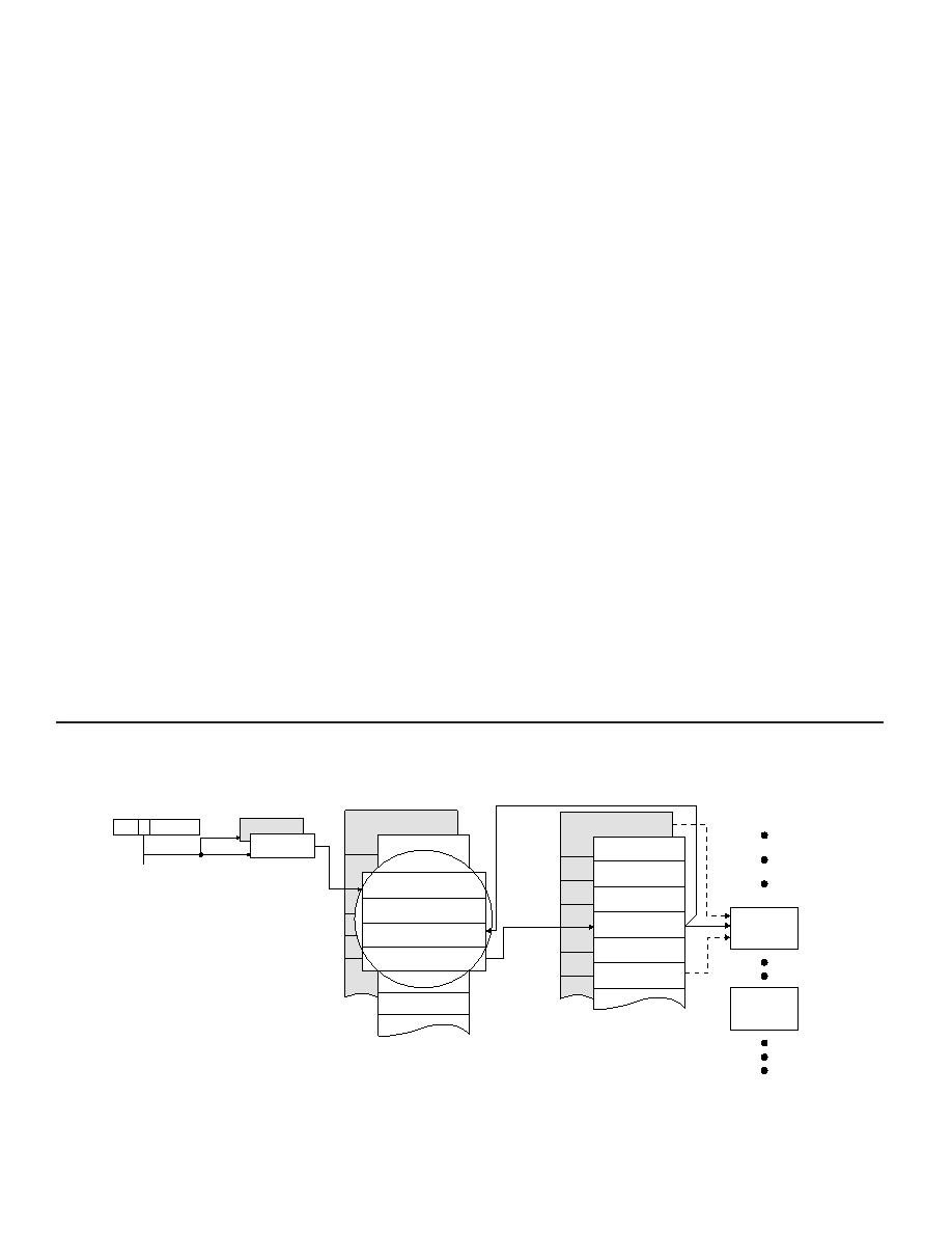
The operation of the single buffered RT mode is illustrated in
FIGURE 6. In the single buffered mode, the respective lookup
table entry must be written by the host processor. Received data
words are written to, or transmitted data words are read from the
data word block with starting address referenced by the lookup
table pointer. In the single buffered mode, the current lookup
table pointer is not updated by the Mini-ACE Mark3 memory
management logic. Therefore, if a subsequent message is
received for the same subaddress, the same Data Word block
will be overwritten or overread.
SUBADDRESS DOUBLE BUFFERING MODE
The Mini-ACE Mark3 provides a double buffering mechanism for
received data, that may be selected on an individual subaddress
basis for any or all receive (and/or broadcast) subaddresses. This
is illustrated in FIGURE 7. It should be noted that the Subaddress
Double Buffering mode is applicable for receive data only, not for
transmit data. Double buffering of transmit messages may be
easily implemented by software techniques.
The purpose of the subaddress double buffering mode is to pro-
vide data sample consistency to the host processor. This is
accomplished by allocating two 32-word data word blocks for each
individual receive (and/or broadcast receive) subaddress. At any
given time, one of the blocks will be designated as the "active"
1553 block while the other will be considered as "inactive". The
data words for the next receive command to that subaddress will
be stored in the active block. Following receipt of a valid message,
the Mini-ACE Mark3 will automatically switch the active and inac-
tive blocks for that subaddress. As a result, the latest, valid, com-
plete data block is always accessible to the host processor.
CIRCULAR BUFFER MODE
The operation of the Mini-ACE Mark3's circular buffer RT mem-
ory management mode is illustrated in FIGURE 8. As in the sin-
gle buffered and double buffered modes, the individual lookup
table entries are initially loaded by the host processor. At the
start of each message, the lookup table entry is stored in the
third position of the respective message block descriptor in the
descriptor stack area of RAM. Receive or transmit data words
are transferred to (from) the circular buffer, starting at the loca-
tion referenced by the lookup table pointer.
In general, the location after the last data word written or read
(modulo the circular buffer size) during the message is written to
the respective lookup table location during the end-of-message
sequence. By so doing, data for the next message for the respec-
tive transmit, receive(/broadcast), or broadcast subaddress will
be accessed from the next lower contiguous block of locations in
the circular buffer.
For the case of a receive (or broadcast receive) message with a
data word error, there is an option such that the lookup table
pointer will only be updated following receipt of a valid message.
That is, the pointer will not be updated following receipt of a
message with an error in a data word. This allows failed mes-
sages in a bulk data transfer to be retried without disrupting the
circular buffer data structure, and without intervention by the
RT's host processor.
GLOBAL CIRCULAR BUFFER
Beyond the programmable choice of single buffer mode, double
buffer mode, or circular buffer mode, programmable on an individ-
ual subaddress basis, the Mini-ACE Mark3 RT architecture pro-
FIGURE 6. RT SINGLE BUFFERED MODE
DATA
BLOCKS
DATA BLOCK
BLOCK STATUS WORD
TIME TAG WORD
DATA BLOCK POINTER
RECEIVED COMMAND
WORD
DESCRIPTOR
STACKS
LOOK-UP
TABLE ADDR
LOOK-UP TABLE
(DATA BLOCK ADDR)
15
13
0
CURRENT
AREA B/A
CONFIGURATION
REGISTER
STACK
POINTERS
(See note)
Note: Lookup table is not used for mode commands when enhanced mode codes are enabled.
相关PDF资料 |
PDF描述 |
|---|---|
| A42MX36-2PQ100B | 40MX and 42MX FPGA Families |
| A42MX36-2PQ100ES | 40MX and 42MX FPGA Families |
| A42MX36-2TQ100 | 40MX and 42MX FPGA Families |
| A42MX36-2TQ100A | 40MX and 42MX FPGA Families |
| A42MX36-2TQ100B | 40MX and 42MX FPGA Families |
相关代理商/技术参数 |
参数描述 |
|---|---|
| A42MX24-FPL84 | 功能描述:IC FPGA MX SGL CHIP 36K 84-PLCC RoHS:否 类别:集成电路 (IC) >> 嵌入式 - FPGA(现场可编程门阵列) 系列:MX 标准包装:40 系列:SX-A LAB/CLB数:6036 逻辑元件/单元数:- RAM 位总计:- 输入/输出数:360 门数:108000 电源电压:2.25 V ~ 5.25 V 安装类型:表面贴装 工作温度:0°C ~ 70°C 封装/外壳:484-BGA 供应商设备封装:484-FPBGA(27X27) |
| A42MX24-FPLG84 | 功能描述:IC FPGA MX SGL CHIP 36K 84-PLCC RoHS:是 类别:集成电路 (IC) >> 嵌入式 - FPGA(现场可编程门阵列) 系列:MX 标准包装:40 系列:SX-A LAB/CLB数:6036 逻辑元件/单元数:- RAM 位总计:- 输入/输出数:360 门数:108000 电源电压:2.25 V ~ 5.25 V 安装类型:表面贴装 工作温度:0°C ~ 70°C 封装/外壳:484-BGA 供应商设备封装:484-FPBGA(27X27) |
| A42MX24-FPQ160 | 功能描述:IC FPGA MX SGL CHIP 36K 160-PQFP RoHS:否 类别:集成电路 (IC) >> 嵌入式 - FPGA(现场可编程门阵列) 系列:MX 标准包装:40 系列:SX-A LAB/CLB数:6036 逻辑元件/单元数:- RAM 位总计:- 输入/输出数:360 门数:108000 电源电压:2.25 V ~ 5.25 V 安装类型:表面贴装 工作温度:0°C ~ 70°C 封装/外壳:484-BGA 供应商设备封装:484-FPBGA(27X27) |
| A42MX24-FPQ208 | 功能描述:IC FPGA MX SGL CHIP 36K 160-PQFP RoHS:否 类别:集成电路 (IC) >> 嵌入式 - FPGA(现场可编程门阵列) 系列:MX 标准包装:40 系列:SX-A LAB/CLB数:6036 逻辑元件/单元数:- RAM 位总计:- 输入/输出数:360 门数:108000 电源电压:2.25 V ~ 5.25 V 安装类型:表面贴装 工作温度:0°C ~ 70°C 封装/外壳:484-BGA 供应商设备封装:484-FPBGA(27X27) |
| A42MX24-FPQG160 | 功能描述:IC FPGA MX SGL CHIP 36K 160-PQFP RoHS:是 类别:集成电路 (IC) >> 嵌入式 - FPGA(现场可编程门阵列) 系列:MX 标准包装:40 系列:SX-A LAB/CLB数:6036 逻辑元件/单元数:- RAM 位总计:- 输入/输出数:360 门数:108000 电源电压:2.25 V ~ 5.25 V 安装类型:表面贴装 工作温度:0°C ~ 70°C 封装/外壳:484-BGA 供应商设备封装:484-FPBGA(27X27) |
发布紧急采购,3分钟左右您将得到回复。