- 您现在的位置:买卖IC网 > PDF目录298744 > A42MX24-3VQ100B (Electronic Theatre Controls, Inc.) 40MX and 42MX FPGA Families PDF资料下载
参数资料
| 型号: | A42MX24-3VQ100B |
| 厂商: | Electronic Theatre Controls, Inc. |
| 英文描述: | 40MX and 42MX FPGA Families |
| 中文描述: | 40MX和42MX FPGA系列 |
| 文件页数: | 49/93页 |
| 文件大小: | 854K |
| 代理商: | A42MX24-3VQ100B |
第1页第2页第3页第4页第5页第6页第7页第8页第9页第10页第11页第12页第13页第14页第15页第16页第17页第18页第19页第20页第21页第22页第23页第24页第25页第26页第27页第28页第29页第30页第31页第32页第33页第34页第35页第36页第37页第38页第39页第40页第41页第42页第43页第44页第45页第46页第47页第48页当前第49页第50页第51页第52页第53页第54页第55页第56页第57页第58页第59页第60页第61页第62页第63页第64页第65页第66页第67页第68页第69页第70页第71页第72页第73页第74页第75页第76页第77页第78页第79页第80页第81页第82页第83页第84页第85页第86页第87页第88页第89页第90页第91页第92页第93页
53
Data Device Corporation
www.ddc-web.com
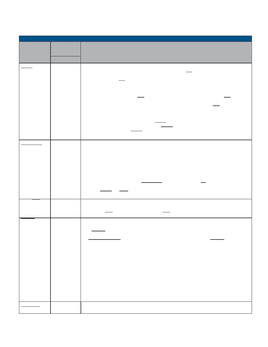
BU-6474X/6484X/6486X
J-07/05-0
POL_SEL (I) /
DTACK (O)
35
Data Transfer Acknowledge or Polarity Select.
In 16-bit buffered mode, if POL_SEL is connected to logic "1", RD/WR should be asserted high (logic "1")
for a read operation and low (logic "0") for a write operation. In 16-bit buffered mode, if POL_SEL is con-
nected to logic "0", RD/WR should be asserted low (logic "0") for a read operation and high (logic "1") for a
write operation.
In 8-bit buffered mode (TRANSPARENT/ BUFFERED = "0" and 16/8 = "0"), POL_SEL input signal used to
control the logic sense of the MSB/LSB signal. If POL_SEL is connected to logic "0", MSB/LSB should be
asserted low (logic "0") to indicate the transfer of the least significant byte and high (logic "1") to indicate
the transfer of the most significant byte. If POL_SEL is connected to logic "1", MSB/LSB should be asserted
high (logic "1") to indicate the transfer of the least significant byte and low (logic "0") to indicate the transfer
of the most significant byte.
In transparent mode, active low output signal (DTACK) used to indicate acceptance of the processor/RAM
interface bus in response to a data transfer grant (DTGRT). Mark3 RAM transfers over A15-A0 and D15-D0
will be framed by the time that DTACK is asserted low.
TRIG_SEL (I) /
MEMENA_IN (I)
34
Memory Enable or Trigger Select input.
In 8-bit buffered mode, input signal (TRIG-SEL) used to select the order in which byte pairs are transferred
to or from the Mark3 by the host processor. In the 8-bit buffered mode, TRIG_SEL should be asserted high
(logic 1) if the byte order for both read operations and write operations is MSB followed by LSB. TRIG_SEL
should be asserted low (logic 0) if the byte order for both read operations and write operations is LSB fol-
lowed by MSB.
This signal has no operation in the 16-bit buffered mode (it does not need to be connected).
In transparent mode, active low input MEMENA_IN, used as a Chip Select (CS) input to the Mark3's inter-
nal shared RAM. If only internal RAM is used, should be connected directly to the output of a gate that is
OR'ing the DTACK and IOEN output signals.
MEM / REG(I)
6
Memory/Register.
Generally connected to either a CPU address line or address decoder output. Selects between memory
access (MEM/REG = "1") or register access (MEM/REG = "0").
TRANSPARENT/
BUFFERED (I)
61
Used to select between the buffered mode (when strapped to logic "0") and transparent/DMA mode (when
strapped to logic "1") for the host processor interface.
SSFLAG (I) /
EXT_TRIG(I)
37
Subsystem Flag (RT) or External Trigger (BC/Word Monitor) input.
In RT mode, if this input is asserted low, the Subsystem Flag bit will be set in the Mark3's RT Status Word.
If the SSFLAG input is logic "0" while bit 8 of Configuration Register #1 has been programmed to logic "1"
(cleared), the Subsystem Flag RT Status Word bit will become logic "1," but bit 8 of Configuration Register
#1, SUBSYSTEM FLAG, will return logic "1" when read. That is, the sense on the SSFLAG input has no
effect on the SUBSYSTEM FLAG register bit.
In the non-enhanced BC mode, this signal operates as an External Trigger input. In BC mode, if the exter-
nal BC Start option is enabled (bit 7 of Configuration Register #1), a low to high transition on this input will
issue a BC Start command, starting execution of the current BC frame.
In the enhanced BC mode, during the execution of a Wait for External Trigger (WTG) instruction, the Mark3
BC will wait for a low-to-high transition on EXT_TRIG before proceeding to the next instruction.
In the Word Monitor mode, if the external trigger is enabled (bit 7 of Configuration Register #1), a low to
high transition on this input will initiate a monitor start.
This input has no effect in Message Monitor mode.
TABLE 53. PROCESSOR INTERFACE CONTROL (CONT.)
SIGNAL NAME
DESCRIPTION
BU-6474XF/GX
BU-6484XF/GX
BU-64863F/GX
PIN
FLAT PACK AND GULL WING PACKAGES - SIGNAL DESCRIPTIONS BY FUNCTIONAL GROUPS (CONT.)
相关PDF资料 |
PDF描述 |
|---|---|
| A42MX36-2PQ100B | 40MX and 42MX FPGA Families |
| A42MX36-2PQ100ES | 40MX and 42MX FPGA Families |
| A42MX36-2TQ100 | 40MX and 42MX FPGA Families |
| A42MX36-2TQ100A | 40MX and 42MX FPGA Families |
| A42MX36-2TQ100B | 40MX and 42MX FPGA Families |
相关代理商/技术参数 |
参数描述 |
|---|---|
| A42MX24-FPL84 | 功能描述:IC FPGA MX SGL CHIP 36K 84-PLCC RoHS:否 类别:集成电路 (IC) >> 嵌入式 - FPGA(现场可编程门阵列) 系列:MX 标准包装:40 系列:SX-A LAB/CLB数:6036 逻辑元件/单元数:- RAM 位总计:- 输入/输出数:360 门数:108000 电源电压:2.25 V ~ 5.25 V 安装类型:表面贴装 工作温度:0°C ~ 70°C 封装/外壳:484-BGA 供应商设备封装:484-FPBGA(27X27) |
| A42MX24-FPLG84 | 功能描述:IC FPGA MX SGL CHIP 36K 84-PLCC RoHS:是 类别:集成电路 (IC) >> 嵌入式 - FPGA(现场可编程门阵列) 系列:MX 标准包装:40 系列:SX-A LAB/CLB数:6036 逻辑元件/单元数:- RAM 位总计:- 输入/输出数:360 门数:108000 电源电压:2.25 V ~ 5.25 V 安装类型:表面贴装 工作温度:0°C ~ 70°C 封装/外壳:484-BGA 供应商设备封装:484-FPBGA(27X27) |
| A42MX24-FPQ160 | 功能描述:IC FPGA MX SGL CHIP 36K 160-PQFP RoHS:否 类别:集成电路 (IC) >> 嵌入式 - FPGA(现场可编程门阵列) 系列:MX 标准包装:40 系列:SX-A LAB/CLB数:6036 逻辑元件/单元数:- RAM 位总计:- 输入/输出数:360 门数:108000 电源电压:2.25 V ~ 5.25 V 安装类型:表面贴装 工作温度:0°C ~ 70°C 封装/外壳:484-BGA 供应商设备封装:484-FPBGA(27X27) |
| A42MX24-FPQ208 | 功能描述:IC FPGA MX SGL CHIP 36K 160-PQFP RoHS:否 类别:集成电路 (IC) >> 嵌入式 - FPGA(现场可编程门阵列) 系列:MX 标准包装:40 系列:SX-A LAB/CLB数:6036 逻辑元件/单元数:- RAM 位总计:- 输入/输出数:360 门数:108000 电源电压:2.25 V ~ 5.25 V 安装类型:表面贴装 工作温度:0°C ~ 70°C 封装/外壳:484-BGA 供应商设备封装:484-FPBGA(27X27) |
| A42MX24-FPQG160 | 功能描述:IC FPGA MX SGL CHIP 36K 160-PQFP RoHS:是 类别:集成电路 (IC) >> 嵌入式 - FPGA(现场可编程门阵列) 系列:MX 标准包装:40 系列:SX-A LAB/CLB数:6036 逻辑元件/单元数:- RAM 位总计:- 输入/输出数:360 门数:108000 电源电压:2.25 V ~ 5.25 V 安装类型:表面贴装 工作温度:0°C ~ 70°C 封装/外壳:484-BGA 供应商设备封装:484-FPBGA(27X27) |
发布紧急采购,3分钟左右您将得到回复。