- 您现在的位置:买卖IC网 > PDF目录12015 > ADUC834BSZ (Analog Devices Inc)IC ADC DUAL16/24BIT W/MCU 52MQFP PDF资料下载
参数资料
| 型号: | ADUC834BSZ |
| 厂商: | Analog Devices Inc |
| 文件页数: | 28/80页 |
| 文件大小: | 0K |
| 描述: | IC ADC DUAL16/24BIT W/MCU 52MQFP |
| 产品培训模块: | Process Control |
| 标准包装: | 1 |
| 系列: | MicroConverter® ADuC8xx |
| 核心处理器: | 8052 |
| 芯体尺寸: | 8-位 |
| 速度: | 12.58MHz |
| 连通性: | EBI/EMI,I²C,SPI,UART/USART |
| 外围设备: | POR,PSM,PWM,温度传感器,WDT |
| 输入/输出数: | 34 |
| 程序存储器容量: | 62KB(62K x 8) |
| 程序存储器类型: | 闪存 |
| EEPROM 大小: | 4K x 8 |
| RAM 容量: | 2.25K x 8 |
| 电压 - 电源 (Vcc/Vdd): | 2.7 V ~ 5.25 V |
| 数据转换器: | A/D 3x16b,4x24b; D/A 1x12b |
| 振荡器型: | 内部 |
| 工作温度: | -40°C ~ 125°C |
| 封装/外壳: | 52-QFP |
| 包装: | 托盘 |
| 产品目录页面: | 738 (CN2011-ZH PDF) |
第1页第2页第3页第4页第5页第6页第7页第8页第9页第10页第11页第12页第13页第14页第15页第16页第17页第18页第19页第20页第21页第22页第23页第24页第25页第26页第27页当前第28页第29页第30页第31页第32页第33页第34页第35页第36页第37页第38页第39页第40页第41页第42页第43页第44页第45页第46页第47页第48页第49页第50页第51页第52页第53页第54页第55页第56页第57页第58页第59页第60页第61页第62页第63页第64页第65页第66页第67页第68页第69页第70页第71页第72页第73页第74页第75页第76页第77页第78页第79页第80页
REV. A
–34–
ADuC834
DAC
The ADuC834 incorporates a 12-bit, voltage output DAC
on-chip. It has a rail-to-rail voltage output buffer capable of driving
10 k
/100 pF. It has two selectable ranges, 0 V to VREF (the inter-
nal bandgap 2.5 V reference) and 0 V to AVDD. It can operate in
12-bit or 8-bit mode. The DAC has a control register, DACCON,
and two data registers, DACH/L. The DAC output can be
programmed to appear at Pin 3 or Pin 12. It should be noted
that in 12-bit mode, the DAC voltage output will be updated as
soon as the DACL data SFR has been written; therefore, the
DAC data registers should be updated as DACH first, followed
by DACL. The 12-bit DAC data should be written into DACH/L
right-justified such that DACL contains the lower eight bits,
and the lower nibble of DACH contains the upper four bits.
Table XV. DACCON SFR Bit Designations
Bit
Name
Description
7
–––
Reserved for Future Use
6
–––
Reserved for Future Use
5
–––
Reserved for Future Use
4
DACPIN
DAC Output Pin Select.
Set by the user to direct the DAC output to Pin 12 (P1.7/AIN4/DAC).
Cleared by user to direct the DAC output to Pin 3 (P1.2/DAC/IEXC1).
3
DAC8
DAC 8-bit Mode Bit.
Set by user to enable 8-bit DAC operation. In this mode, the 8-bits in DACL SFR are routed
to the 8 MSBs of the DAC, and the 4 LSBs of the DAC are set to zero.
Cleared by user to operate the DAC in its normal 12-bit mode of operation.
2
DACRN
DAC Output Range Bit.
Set by user to configure DAC range of 0–AVDD.
Cleared by user to configure DAC range of 0 V–2.5 V (VREF).
1
DACCLR
DAC Clear Bit.
Set to 1 by user to enable normal DAC operation.
Cleared to 0 by user to reset DAC data registers DACL/H to zero.
0
DACEN
DAC Enable Bit.
Set to 1 by user to enable normal DAC operation.
Cleared to 0 by user to power down the DAC.
DACH/L
DAC Data Registers
Function
DAC Data Registers, written by user to update the DAC output.
SFR Address
DACL (DAC Data Low Byte)
FBH
DACH (DAC Data High Byte)
FCH
Power-On Default Value
00H
Both Registers
Bit Addressable
No
Both Registers
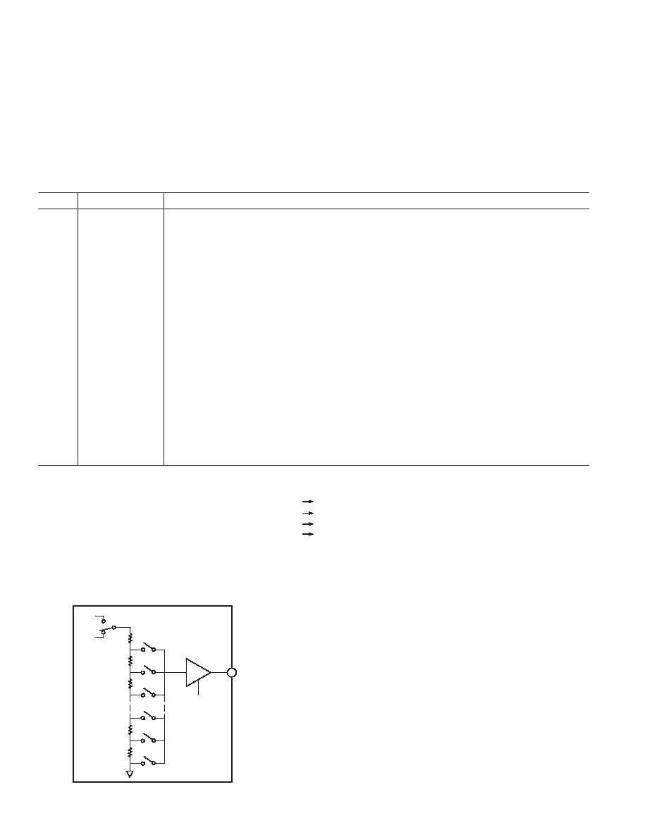
Using the D/A Converter
The on-chip D/A converter architecture consists of a resistor
string DAC followed by an output buffer amplifier, the func-
tional equivalent of which is illustrated in Figure 21.
R
ADuC834
AVDD
VREF
OUTPUT
BUFFER
DAC
12
HIGH-Z
DISABLE
(FROM MCU)
Figure 21. Resistor String DAC Functional Equivalent
Features of this architecture include inherent guaranteed mono-
tonicity and excellent differential linearity. As illustrated in
Figure 21, the reference source for the DAC is user selectable in
software. It can be either AVDD or VREF. In 0-to-AVDD mode,
the DAC output transfer function spans from 0 V to the voltage
at the AVDD pin. In 0-to-VREF mode, the DAC output transfer
function spans from 0 V to the internal VREF (2.5 V). The DAC
output buffer amplifier features a true rail-to-rail output stage
implementation. This means that, unloaded, each output is
capable of swinging to within less than 100 mV of both AVDD
and ground. Moreover, the DAC’s linearity specification (when
driving a 10 k
resistive load to ground) is guaranteed through
the full transfer function except codes 0 to 48 in 0-to-VREF
mode and 0 to 100 and 3950 to 4095 in 0-to-VDD mode.
Linearity degradation near ground and VDD is caused by saturation
of the output amplifier, and a general representation of its effects
(neglecting offset and gain error) is illustrated in Figure 22. The
dotted line in Figure 22 indicates the ideal transfer function, and
the solid line represents what the transfer function might look
like with endpoint nonlinearities due to saturation of the output
amplifier.
相关PDF资料 |
PDF描述 |
|---|---|
| VI-JVP-IY-F2 | CONVERTER MOD DC/DC 13.8V 50W |
| VE-B3D-IY-F2 | CONVERTER MOD DC/DC 85V 50W |
| AT91SAM9XE256-QU | MCU ARM9 256K FLASH 208-PQFP |
| VI-JVN-IY-F4 | CONVERTER MOD DC/DC 18.5V 50W |
| VI-JVM-IY-F2 | CONVERTER MOD DC/DC 10V 50W |
相关代理商/技术参数 |
参数描述 |
|---|---|
| ADUC836 | 制造商:AD 制造商全称:Analog Devices 功能描述:MicroConverter, Dual 16-Bit-ADCs with Embedded 62 kB Flash MCU |
| ADUC836_02 | 制造商:AD 制造商全称:Analog Devices 功能描述:MicroConverter, Dual 16-Bit ADCs with Embedded 62 kB Flash MCU |
| ADUC836BCP | 制造商:Rochester Electronics LLC 功能描述: 制造商:Analog Devices 功能描述: |
| ADUC836BCPZ | 功能描述:IC MCU 62K FLASH ADC/DAC 56LFCSP RoHS:是 类别:集成电路 (IC) >> 嵌入式 - 微控制器, 系列:MicroConverter® ADuC8xx 标准包装:38 系列:Encore!® XP® 核心处理器:eZ8 芯体尺寸:8-位 速度:5MHz 连通性:IrDA,UART/USART 外围设备:欠压检测/复位,LED,POR,PWM,WDT 输入/输出数:16 程序存储器容量:4KB(4K x 8) 程序存储器类型:闪存 EEPROM 大小:- RAM 容量:1K x 8 电压 - 电源 (Vcc/Vdd):2.7 V ~ 3.6 V 数据转换器:- 振荡器型:内部 工作温度:-40°C ~ 105°C 封装/外壳:20-SOIC(0.295",7.50mm 宽) 包装:管件 其它名称:269-4116Z8F0413SH005EG-ND |
| ADUC836BCPZ-REEL | 功能描述:IC MCU 62K FLASH ADC/DAC 56LFCSP RoHS:是 类别:集成电路 (IC) >> 嵌入式 - 微控制器, 系列:MicroConverter® ADuC8xx 标准包装:38 系列:Encore!® XP® 核心处理器:eZ8 芯体尺寸:8-位 速度:5MHz 连通性:IrDA,UART/USART 外围设备:欠压检测/复位,LED,POR,PWM,WDT 输入/输出数:16 程序存储器容量:4KB(4K x 8) 程序存储器类型:闪存 EEPROM 大小:- RAM 容量:1K x 8 电压 - 电源 (Vcc/Vdd):2.7 V ~ 3.6 V 数据转换器:- 振荡器型:内部 工作温度:-40°C ~ 105°C 封装/外壳:20-SOIC(0.295",7.50mm 宽) 包装:管件 其它名称:269-4116Z8F0413SH005EG-ND |
发布紧急采购,3分钟左右您将得到回复。