- 您现在的位置:买卖IC网 > PDF目录12015 > ADUC834BSZ (Analog Devices Inc)IC ADC DUAL16/24BIT W/MCU 52MQFP PDF资料下载
参数资料
| 型号: | ADUC834BSZ |
| 厂商: | Analog Devices Inc |
| 文件页数: | 60/80页 |
| 文件大小: | 0K |
| 描述: | IC ADC DUAL16/24BIT W/MCU 52MQFP |
| 产品培训模块: | Process Control |
| 标准包装: | 1 |
| 系列: | MicroConverter® ADuC8xx |
| 核心处理器: | 8052 |
| 芯体尺寸: | 8-位 |
| 速度: | 12.58MHz |
| 连通性: | EBI/EMI,I²C,SPI,UART/USART |
| 外围设备: | POR,PSM,PWM,温度传感器,WDT |
| 输入/输出数: | 34 |
| 程序存储器容量: | 62KB(62K x 8) |
| 程序存储器类型: | 闪存 |
| EEPROM 大小: | 4K x 8 |
| RAM 容量: | 2.25K x 8 |
| 电压 - 电源 (Vcc/Vdd): | 2.7 V ~ 5.25 V |
| 数据转换器: | A/D 3x16b,4x24b; D/A 1x12b |
| 振荡器型: | 内部 |
| 工作温度: | -40°C ~ 125°C |
| 封装/外壳: | 52-QFP |
| 包装: | 托盘 |
| 产品目录页面: | 738 (CN2011-ZH PDF) |
第1页第2页第3页第4页第5页第6页第7页第8页第9页第10页第11页第12页第13页第14页第15页第16页第17页第18页第19页第20页第21页第22页第23页第24页第25页第26页第27页第28页第29页第30页第31页第32页第33页第34页第35页第36页第37页第38页第39页第40页第41页第42页第43页第44页第45页第46页第47页第48页第49页第50页第51页第52页第53页第54页第55页第56页第57页第58页第59页当前第60页第61页第62页第63页第64页第65页第66页第67页第68页第69页第70页第71页第72页第73页第74页第75页第76页第77页第78页第79页第80页
REV. A
ADuC834
–63–
ADuC834 HARDWARE DESIGN CONSIDERATIONS
This section outlines some of the key hardware design consider-
ations that must be addressed when integrating the ADuC834
into any hardware system.
External Memory Interface
In addition to its internal program and data memories, the
ADuC834 can access up to 64 Kbytes of external program memory
(ROM/PROM/and so on) and up to 16 Mbytes of external data
memory (SRAM).
To select from which code space (internal or external program
memory) to begin executing code, tie the
EA (external access)
pin high or low, respectively. When
EA is high (pulled up to
VDD), user program execution will start at Address 0 in the
internal 62 Kbytes Flash/EE code space. When
EA is low (tied
to ground) user program execution will start at Address 0 in the
external code space. When executing from internal code space,
accesses to the program space above F7FFH (62 Kbytes) will be
read as NOP instructions.
Note that a second very important function of the
EA pin is
described in the Single Pin Emulation Mode section.
External program memory (if used) must be connected to
the ADuC834 as illustrated in Figure 58. Sixteen I/O lines
(Ports 0 and 2) are dedicated to bus functions during external
program memory fetches. Port 0 (P0) serves as a multiplexed
address/databus. It emits the low byte of the program counter
(PCL) as an address, and then goes into a high impedance input
state awaiting the arrival of the code byte from the program
memory. During the time that the low byte of the program counter
is valid on P0, the signal ALE (Address Latch Enable) clocks
this byte into an external address latch. Meanwhile, Port 2 (P2)
emits the high byte of the program counter (PCH), and
PSEN
strobes the EPROM and the code byte is read into the ADuC834.
LATCH
EPROM
OE
A8–A15
A0–A7
D0–D7
(INSTRUCTION)
ADuC834
PSEN
P2
ALE
P0
Figure 58. External Program Memory Interface
Note that program memory addresses are always 16 bits wide,
even in cases where the actual amount of program memory used
is less than 64 Kbytes. External program execution sacrifices two
of the 8-bit ports (P0 and P2) to the function of addressing the
program memory. While executing from external program memory,
Ports 0 and 2 can be used simultaneously for read/write access
to external data memory, but not for general-purpose I/O.
Though both external program memory and external data
memory are accessed using some of the same pins, the two are
completely independent of each other from a software point of
view. For example, the chip can read/write external data memory
while executing from external program memory.
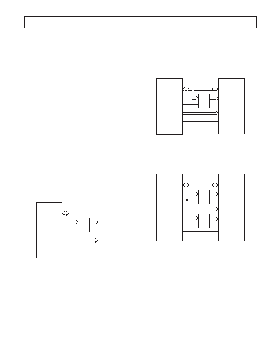
Figure 59 shows a hardware configuration for accessing up to
64 Kbytes of external data memory. This interface is standard
to any 8051 compatible MCU.
LATCH
SRAM
OE
A8–A15
A0–A7
D0–D7
(DATA)
ADuC834
RD
P2
ALE
P0
WE
WR
Figure 59. External Data Memory Interface
(64 Kbytes Address Space)
If access to more than 64 Kbytes of RAM is desired, a feature
unique to the MicroConverter allows addressing up to 16 Mbytes
of external RAM simply by adding an additional latch as illus-
trated in Figure 60.
LATCH
ADuC834
RD
P2
ALE
P0
WR
LATCH
SRAM
OE
A8–A15
A0–A7
D0–D7
(DATA)
WE
A16–A23
Figure 60. External Data Memory Interface
(16 Mbytes Address Space)
In either implementation, Port 0 (P0) serves as a multiplexed
address/databus. It emits the low byte of the data pointer (DPL)
as an address, which is latched by ALE prior to data being placed
on the bus by the ADuC834 (write operation) or the external
data memory (read operation). Port 2 (P2) provides the data
pointer page byte (DPP) to be latched by ALE, followed by the
data pointer high byte (DPH). If no latch is connected to P2,
DPP is ignored by the SRAM, and the 8051 standard of 64 Kbyte
external data memory access is maintained.
Detailed timing diagrams of external program and data memory
read and write access can be found in the Timing Specification
sections of this data sheet.
相关PDF资料 |
PDF描述 |
|---|---|
| VI-JVP-IY-F2 | CONVERTER MOD DC/DC 13.8V 50W |
| VE-B3D-IY-F2 | CONVERTER MOD DC/DC 85V 50W |
| AT91SAM9XE256-QU | MCU ARM9 256K FLASH 208-PQFP |
| VI-JVN-IY-F4 | CONVERTER MOD DC/DC 18.5V 50W |
| VI-JVM-IY-F2 | CONVERTER MOD DC/DC 10V 50W |
相关代理商/技术参数 |
参数描述 |
|---|---|
| ADUC836 | 制造商:AD 制造商全称:Analog Devices 功能描述:MicroConverter, Dual 16-Bit-ADCs with Embedded 62 kB Flash MCU |
| ADUC836_02 | 制造商:AD 制造商全称:Analog Devices 功能描述:MicroConverter, Dual 16-Bit ADCs with Embedded 62 kB Flash MCU |
| ADUC836BCP | 制造商:Rochester Electronics LLC 功能描述: 制造商:Analog Devices 功能描述: |
| ADUC836BCPZ | 功能描述:IC MCU 62K FLASH ADC/DAC 56LFCSP RoHS:是 类别:集成电路 (IC) >> 嵌入式 - 微控制器, 系列:MicroConverter® ADuC8xx 标准包装:38 系列:Encore!® XP® 核心处理器:eZ8 芯体尺寸:8-位 速度:5MHz 连通性:IrDA,UART/USART 外围设备:欠压检测/复位,LED,POR,PWM,WDT 输入/输出数:16 程序存储器容量:4KB(4K x 8) 程序存储器类型:闪存 EEPROM 大小:- RAM 容量:1K x 8 电压 - 电源 (Vcc/Vdd):2.7 V ~ 3.6 V 数据转换器:- 振荡器型:内部 工作温度:-40°C ~ 105°C 封装/外壳:20-SOIC(0.295",7.50mm 宽) 包装:管件 其它名称:269-4116Z8F0413SH005EG-ND |
| ADUC836BCPZ-REEL | 功能描述:IC MCU 62K FLASH ADC/DAC 56LFCSP RoHS:是 类别:集成电路 (IC) >> 嵌入式 - 微控制器, 系列:MicroConverter® ADuC8xx 标准包装:38 系列:Encore!® XP® 核心处理器:eZ8 芯体尺寸:8-位 速度:5MHz 连通性:IrDA,UART/USART 外围设备:欠压检测/复位,LED,POR,PWM,WDT 输入/输出数:16 程序存储器容量:4KB(4K x 8) 程序存储器类型:闪存 EEPROM 大小:- RAM 容量:1K x 8 电压 - 电源 (Vcc/Vdd):2.7 V ~ 3.6 V 数据转换器:- 振荡器型:内部 工作温度:-40°C ~ 105°C 封装/外壳:20-SOIC(0.295",7.50mm 宽) 包装:管件 其它名称:269-4116Z8F0413SH005EG-ND |
发布紧急采购,3分钟左右您将得到回复。