- 您现在的位置:买卖IC网 > PDF目录12015 > ADUC834BSZ (Analog Devices Inc)IC ADC DUAL16/24BIT W/MCU 52MQFP PDF资料下载
参数资料
| 型号: | ADUC834BSZ |
| 厂商: | Analog Devices Inc |
| 文件页数: | 61/80页 |
| 文件大小: | 0K |
| 描述: | IC ADC DUAL16/24BIT W/MCU 52MQFP |
| 产品培训模块: | Process Control |
| 标准包装: | 1 |
| 系列: | MicroConverter® ADuC8xx |
| 核心处理器: | 8052 |
| 芯体尺寸: | 8-位 |
| 速度: | 12.58MHz |
| 连通性: | EBI/EMI,I²C,SPI,UART/USART |
| 外围设备: | POR,PSM,PWM,温度传感器,WDT |
| 输入/输出数: | 34 |
| 程序存储器容量: | 62KB(62K x 8) |
| 程序存储器类型: | 闪存 |
| EEPROM 大小: | 4K x 8 |
| RAM 容量: | 2.25K x 8 |
| 电压 - 电源 (Vcc/Vdd): | 2.7 V ~ 5.25 V |
| 数据转换器: | A/D 3x16b,4x24b; D/A 1x12b |
| 振荡器型: | 内部 |
| 工作温度: | -40°C ~ 125°C |
| 封装/外壳: | 52-QFP |
| 包装: | 托盘 |
| 产品目录页面: | 738 (CN2011-ZH PDF) |
第1页第2页第3页第4页第5页第6页第7页第8页第9页第10页第11页第12页第13页第14页第15页第16页第17页第18页第19页第20页第21页第22页第23页第24页第25页第26页第27页第28页第29页第30页第31页第32页第33页第34页第35页第36页第37页第38页第39页第40页第41页第42页第43页第44页第45页第46页第47页第48页第49页第50页第51页第52页第53页第54页第55页第56页第57页第58页第59页第60页当前第61页第62页第63页第64页第65页第66页第67页第68页第69页第70页第71页第72页第73页第74页第75页第76页第77页第78页第79页第80页
REV. A
–64–
ADuC834
Power Supplies
The ADuC834’s operational power supply voltage range is
2.7 V to 5.25 V. Although the guaranteed data sheet specifica-
tions are given only for power supplies within 2.7 V to 3.6 V or
5% of the nominal 5 V level, the chip will function equally well
at any power supply level between 2.7 V and 5.25 V.
Separate analog and digital power supply pins (AVDD and DVDD
respectively) allow AVDD to be kept relatively free of noisy digi-
tal signals often present on the system DVDD line. In this mode,
the part can also operate with split supplies; that is, using differ-
ent voltage supply levels for each supply. For example, this
means that the system can be designed to operate with a DVDD
voltage level of 3 V while the AVDD level can be at 5 V, or vice-
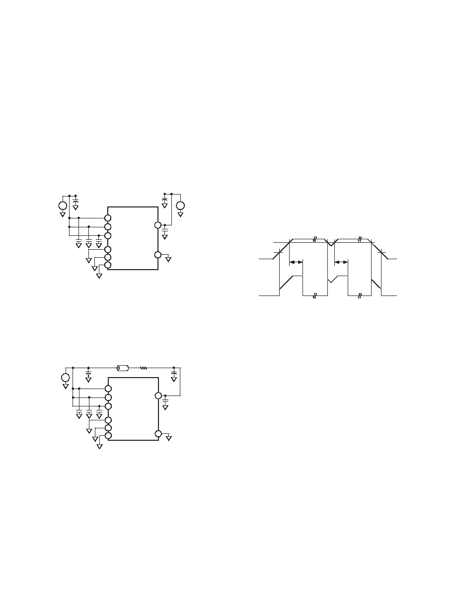
versa if required. A typical split supply configuration is shown in
Figure 61.
DVDD
48
34
20
ADuC834
5
6
AGND
AVDD
–
+
0.1 F
10 F
ANALOG SUPPLY
10 F
DGND
35
21
47
0.1 F
DIGITAL SUPPLY
–
+
Figure 61. External Dual Supply Connections
As an alternative to providing two separate power supplies,
AVDD can be kept quiet by placing a small series resistor and/or
ferrite bead between it and DVDD, and then decoupling AVDD
separately to ground. An example of this configuration is shown
in Figure 62. In this configuration, other analog circuitry (such
as op amps, voltage reference, and so on) can be powered from
the AVDD supply line as well.
DVDD
48
34
20
ADuC834
5
6
AGND
AVDD
0.1 F
10 F
DGND
35
21
47
0.1 F
–
+
DIGITAL SUPPLY
10 F
1.6
BEAD
Figure 62. External Single Supply Connections
Notice that in both Figure 61 and Figure 62 a large value (10 F)
reservoir capacitor sits on DVDD and a separate 10 F capacitor
sits on AVDD. Also, local decoupling capacitors (0.1 F) are
located at each VDD pin of the chip. As per standard design
practice, be sure to include all of these capacitors and ensure
the smaller capacitors are closest to each VDD pin with lead
lengths as short as possible. Connect the ground terminal of
each of these capacitors directly to the underlying ground plane.
Finally, it should also be noticed that, at all times, the analog
and digital ground pins on the ADuC834 should be referenced
to the same system ground reference point.
Power-On Reset Operation
An internal POR (Power-On Reset) is implemented on the
ADuC834. For DVDD below 2.45 V, the internal POR will hold
the ADuC834 in reset. As DVDD rises above 2.45 V, an internal
timer will time out for typically 128 ms before the part is
released from reset. The user must ensure that the power supply
has reached a stable 2.7 V minimum level by this time. Likewise
on power-down, the internal POR will hold the ADuC834 in
reset until the power supply has dropped below 1 V. Figure 63
illustrates the operation of the internal POR in detail.
128ms TYP
1.0V TYP
128ms TYP
2.45V TYP
1.0V TYP
INTERNAL
CORE RESET
DVDD
Figure 63. Internal Power-on-Reset Operation
Power Consumption
The DVDD power supply current consumption is specified in
normal, idle, and power-down modes. The AVDD power supply
current is specified with the analog peripherals disabled. The
normal mode power consumption represents the current drawn
from DVDD by the digital core. The other on-chip peripherals
(watchdog timer, power supply monitor, and so on) consume
negligible current and are therefore lumped in with the normal
operating current here. Of course, the user must add any cur-
rents sourced by the parallel and serial I/O pins, and those
sourced by the DAC in order to determine the total current
needed at the ADuC834’s DVDD and AVDD supply pins. Also,
current drawn from the DVDD supply will increase by approxi-
mately 5 mA during Flash/EE erase and program cycles.
相关PDF资料 |
PDF描述 |
|---|---|
| VI-JVP-IY-F2 | CONVERTER MOD DC/DC 13.8V 50W |
| VE-B3D-IY-F2 | CONVERTER MOD DC/DC 85V 50W |
| AT91SAM9XE256-QU | MCU ARM9 256K FLASH 208-PQFP |
| VI-JVN-IY-F4 | CONVERTER MOD DC/DC 18.5V 50W |
| VI-JVM-IY-F2 | CONVERTER MOD DC/DC 10V 50W |
相关代理商/技术参数 |
参数描述 |
|---|---|
| ADUC836 | 制造商:AD 制造商全称:Analog Devices 功能描述:MicroConverter, Dual 16-Bit-ADCs with Embedded 62 kB Flash MCU |
| ADUC836_02 | 制造商:AD 制造商全称:Analog Devices 功能描述:MicroConverter, Dual 16-Bit ADCs with Embedded 62 kB Flash MCU |
| ADUC836BCP | 制造商:Rochester Electronics LLC 功能描述: 制造商:Analog Devices 功能描述: |
| ADUC836BCPZ | 功能描述:IC MCU 62K FLASH ADC/DAC 56LFCSP RoHS:是 类别:集成电路 (IC) >> 嵌入式 - 微控制器, 系列:MicroConverter® ADuC8xx 标准包装:38 系列:Encore!® XP® 核心处理器:eZ8 芯体尺寸:8-位 速度:5MHz 连通性:IrDA,UART/USART 外围设备:欠压检测/复位,LED,POR,PWM,WDT 输入/输出数:16 程序存储器容量:4KB(4K x 8) 程序存储器类型:闪存 EEPROM 大小:- RAM 容量:1K x 8 电压 - 电源 (Vcc/Vdd):2.7 V ~ 3.6 V 数据转换器:- 振荡器型:内部 工作温度:-40°C ~ 105°C 封装/外壳:20-SOIC(0.295",7.50mm 宽) 包装:管件 其它名称:269-4116Z8F0413SH005EG-ND |
| ADUC836BCPZ-REEL | 功能描述:IC MCU 62K FLASH ADC/DAC 56LFCSP RoHS:是 类别:集成电路 (IC) >> 嵌入式 - 微控制器, 系列:MicroConverter® ADuC8xx 标准包装:38 系列:Encore!® XP® 核心处理器:eZ8 芯体尺寸:8-位 速度:5MHz 连通性:IrDA,UART/USART 外围设备:欠压检测/复位,LED,POR,PWM,WDT 输入/输出数:16 程序存储器容量:4KB(4K x 8) 程序存储器类型:闪存 EEPROM 大小:- RAM 容量:1K x 8 电压 - 电源 (Vcc/Vdd):2.7 V ~ 3.6 V 数据转换器:- 振荡器型:内部 工作温度:-40°C ~ 105°C 封装/外壳:20-SOIC(0.295",7.50mm 宽) 包装:管件 其它名称:269-4116Z8F0413SH005EG-ND |
发布紧急采购,3分钟左右您将得到回复。