- 您现在的位置:买卖IC网 > PDF目录12015 > ADUC834BSZ (Analog Devices Inc)IC ADC DUAL16/24BIT W/MCU 52MQFP PDF资料下载
参数资料
| 型号: | ADUC834BSZ |
| 厂商: | Analog Devices Inc |
| 文件页数: | 47/80页 |
| 文件大小: | 0K |
| 描述: | IC ADC DUAL16/24BIT W/MCU 52MQFP |
| 产品培训模块: | Process Control |
| 标准包装: | 1 |
| 系列: | MicroConverter® ADuC8xx |
| 核心处理器: | 8052 |
| 芯体尺寸: | 8-位 |
| 速度: | 12.58MHz |
| 连通性: | EBI/EMI,I²C,SPI,UART/USART |
| 外围设备: | POR,PSM,PWM,温度传感器,WDT |
| 输入/输出数: | 34 |
| 程序存储器容量: | 62KB(62K x 8) |
| 程序存储器类型: | 闪存 |
| EEPROM 大小: | 4K x 8 |
| RAM 容量: | 2.25K x 8 |
| 电压 - 电源 (Vcc/Vdd): | 2.7 V ~ 5.25 V |
| 数据转换器: | A/D 3x16b,4x24b; D/A 1x12b |
| 振荡器型: | 内部 |
| 工作温度: | -40°C ~ 125°C |
| 封装/外壳: | 52-QFP |
| 包装: | 托盘 |
| 产品目录页面: | 738 (CN2011-ZH PDF) |
第1页第2页第3页第4页第5页第6页第7页第8页第9页第10页第11页第12页第13页第14页第15页第16页第17页第18页第19页第20页第21页第22页第23页第24页第25页第26页第27页第28页第29页第30页第31页第32页第33页第34页第35页第36页第37页第38页第39页第40页第41页第42页第43页第44页第45页第46页当前第47页第48页第49页第50页第51页第52页第53页第54页第55页第56页第57页第58页第59页第60页第61页第62页第63页第64页第65页第66页第67页第68页第69页第70页第71页第72页第73页第74页第75页第76页第77页第78页第79页第80页
REV. A
ADuC834
–51–
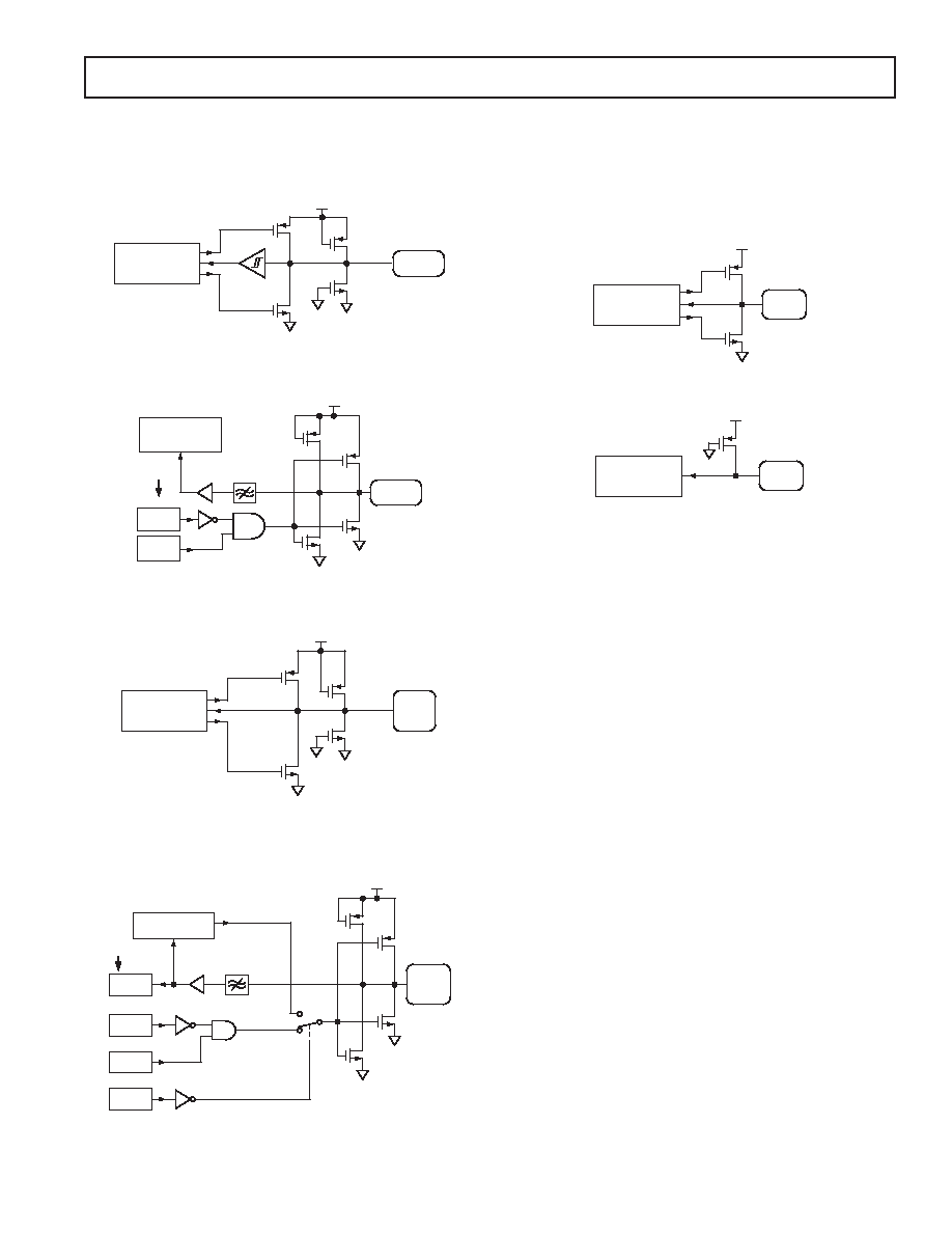
Notice also that direct access to the SCLOCK and SDATA/MOSI
pins is afforded through the SFR interface in I
2C master mode.
Therefore, if you are not using the SPI or I
2C functions, you can
use these two pins to give additional high current digital outputs.
HARDWARE SPI
(MASTER/SLAVE)
Q3
SCHMITT
TRIGGER
Q1
Q2 (OFF)
DVDD
SCLOCK
PIN
Q4 (OFF)
SPE = 1 (SPI ENABLE)
Figure 42. SCLOCK Pin I/O Functional Equivalent in
SPI Mode
MCO
I2CM
SFR
BITS
50ns GLITCH
REJECTION FILTER
HARDWARE I2C
(SLAVE ONLY)
Q3
Q4
SCLOCK
PIN
Q2
Q1
(OFF)
DVDD
SPE = 0 (I2C ENABLE)
Figure 43. SCLOCK Pin I/O Functional Equivalent in
I2C Mode
HARDWARE SPI
(MASTER/SLAVE)
Q3
Q1
Q2 (OFF)
DVDD
SDATA/
MOSI
PIN
Q4 (OFF)
SPE = 1 (SPI ENABLE)
Figure 44. SDATA/MOSI Pin I/O Functional Equivalent
in SPI Mode
Q3
Q4
Q2
Q1
(OFF)
DVDD
MDI
MDO
MDE
I2CM
HARDWARE I2C
(SLAVE ONLY)
50ns GLITCH
REJECTION FILTER
SDATA/
MOSI
PIN
SFR
BITS
SPE = 0 (I2C ENABLE)
Figure 45. SDATA/MOSI Pin I/O Functional Equivalent
in I2C Mode
As shown in Figure 46, the MISO pin in SPI master/slave
operation offers the exact same pull-up and pull-down configu-
ration as the MOSI pin in SPI slave/master operation.
The
SS pin has a weak internal pull-up permanently enabled to
prevent the
SS input from floating. This pull-up can be easily
overdriven by an external device to drive the
SS pin low.
HARDWARE SPI
(MASTER/SLAVE)
MISO
PIN
DVDD
Figure 46. MISO Pin I/O Functional Equivalent
HARDWARE SPI
(MASTER/SLAVE)
SS
PIN
DVDD
Figure 47.
SS Pin I/O Functional Equivalent
Read-Modify-Write Instructions
Some 8051 instructions that read a port read the latch and
others read the pin. The instructions that read the latch rather
than the pins are the ones that read a value, possibly change it,
and then rewrite it to the latch. These are called “read-modify-
write” instructions. Listed below are the read-modify-write
instructions. When the destination operand is a port, or a port
bit, these instructions read the latch rather than the pin.
ANL
(Logical AND, e.g., ANL P1, A)
ORL
(Logical OR, e.g., ORL P2, A)
XRL
(Logical EX-OR, e.g., XRL P3, A)
JBC
(Jump If Bit = 1 and Clear Bit,
e.g., JBC P1.1, LABEL
CPL
(Complement Bit, e.g., CPL P3.0)
INC
(Increment, e.g., INC P2)
DEC
(Decrement, e.g., DEC P2)
DJNZ
(Decrement and Jump IFf Not Zero,
e.g.,DJNZ P3, LABEL)
MOV PX.Y, C* (Move Carry to Bit Y of Port X)
CLR PX.Y*
(Clear Bit Y of Port X)
SETB PX.Y*
(Set Bit Y of Port X)
The reason that read-modify-write instructions are directed to
the latch rather than the pin is to avoid a possible misinterpreta-
tion of the voltage level of a pin. For example, a port pin might
be used to drive the base of a transistor. When a 1 is written to
the bit, the transistor is turned on. If the CPU then reads the
same port bit at the pin rather then the latch, it will read the
base voltage of the transistor and interpret it as a Logic 0. Read-
ing the latch rather than the pin will return the correct value of 1.
*These instruction read the port byte (all 8 bits), modify the addressed bit and
then write the new byte back to the latch.
相关PDF资料 |
PDF描述 |
|---|---|
| VI-JVP-IY-F2 | CONVERTER MOD DC/DC 13.8V 50W |
| VE-B3D-IY-F2 | CONVERTER MOD DC/DC 85V 50W |
| AT91SAM9XE256-QU | MCU ARM9 256K FLASH 208-PQFP |
| VI-JVN-IY-F4 | CONVERTER MOD DC/DC 18.5V 50W |
| VI-JVM-IY-F2 | CONVERTER MOD DC/DC 10V 50W |
相关代理商/技术参数 |
参数描述 |
|---|---|
| ADUC836 | 制造商:AD 制造商全称:Analog Devices 功能描述:MicroConverter, Dual 16-Bit-ADCs with Embedded 62 kB Flash MCU |
| ADUC836_02 | 制造商:AD 制造商全称:Analog Devices 功能描述:MicroConverter, Dual 16-Bit ADCs with Embedded 62 kB Flash MCU |
| ADUC836BCP | 制造商:Rochester Electronics LLC 功能描述: 制造商:Analog Devices 功能描述: |
| ADUC836BCPZ | 功能描述:IC MCU 62K FLASH ADC/DAC 56LFCSP RoHS:是 类别:集成电路 (IC) >> 嵌入式 - 微控制器, 系列:MicroConverter® ADuC8xx 标准包装:38 系列:Encore!® XP® 核心处理器:eZ8 芯体尺寸:8-位 速度:5MHz 连通性:IrDA,UART/USART 外围设备:欠压检测/复位,LED,POR,PWM,WDT 输入/输出数:16 程序存储器容量:4KB(4K x 8) 程序存储器类型:闪存 EEPROM 大小:- RAM 容量:1K x 8 电压 - 电源 (Vcc/Vdd):2.7 V ~ 3.6 V 数据转换器:- 振荡器型:内部 工作温度:-40°C ~ 105°C 封装/外壳:20-SOIC(0.295",7.50mm 宽) 包装:管件 其它名称:269-4116Z8F0413SH005EG-ND |
| ADUC836BCPZ-REEL | 功能描述:IC MCU 62K FLASH ADC/DAC 56LFCSP RoHS:是 类别:集成电路 (IC) >> 嵌入式 - 微控制器, 系列:MicroConverter® ADuC8xx 标准包装:38 系列:Encore!® XP® 核心处理器:eZ8 芯体尺寸:8-位 速度:5MHz 连通性:IrDA,UART/USART 外围设备:欠压检测/复位,LED,POR,PWM,WDT 输入/输出数:16 程序存储器容量:4KB(4K x 8) 程序存储器类型:闪存 EEPROM 大小:- RAM 容量:1K x 8 电压 - 电源 (Vcc/Vdd):2.7 V ~ 3.6 V 数据转换器:- 振荡器型:内部 工作温度:-40°C ~ 105°C 封装/外壳:20-SOIC(0.295",7.50mm 宽) 包装:管件 其它名称:269-4116Z8F0413SH005EG-ND |
发布紧急采购,3分钟左右您将得到回复。