- 您现在的位置:买卖IC网 > PDF目录12015 > ADUC834BSZ (Analog Devices Inc)IC ADC DUAL16/24BIT W/MCU 52MQFP PDF资料下载
参数资料
| 型号: | ADUC834BSZ |
| 厂商: | Analog Devices Inc |
| 文件页数: | 50/80页 |
| 文件大小: | 0K |
| 描述: | IC ADC DUAL16/24BIT W/MCU 52MQFP |
| 产品培训模块: | Process Control |
| 标准包装: | 1 |
| 系列: | MicroConverter® ADuC8xx |
| 核心处理器: | 8052 |
| 芯体尺寸: | 8-位 |
| 速度: | 12.58MHz |
| 连通性: | EBI/EMI,I²C,SPI,UART/USART |
| 外围设备: | POR,PSM,PWM,温度传感器,WDT |
| 输入/输出数: | 34 |
| 程序存储器容量: | 62KB(62K x 8) |
| 程序存储器类型: | 闪存 |
| EEPROM 大小: | 4K x 8 |
| RAM 容量: | 2.25K x 8 |
| 电压 - 电源 (Vcc/Vdd): | 2.7 V ~ 5.25 V |
| 数据转换器: | A/D 3x16b,4x24b; D/A 1x12b |
| 振荡器型: | 内部 |
| 工作温度: | -40°C ~ 125°C |
| 封装/外壳: | 52-QFP |
| 包装: | 托盘 |
| 产品目录页面: | 738 (CN2011-ZH PDF) |
第1页第2页第3页第4页第5页第6页第7页第8页第9页第10页第11页第12页第13页第14页第15页第16页第17页第18页第19页第20页第21页第22页第23页第24页第25页第26页第27页第28页第29页第30页第31页第32页第33页第34页第35页第36页第37页第38页第39页第40页第41页第42页第43页第44页第45页第46页第47页第48页第49页当前第50页第51页第52页第53页第54页第55页第56页第57页第58页第59页第60页第61页第62页第63页第64页第65页第66页第67页第68页第69页第70页第71页第72页第73页第74页第75页第76页第77页第78页第79页第80页
REV. A
–54–
ADuC834
TIMER/COUNTER 0 AND 1 OPERATING MODES
The following paragraphs describe the operating modes for
Timer/Counters 0 and 1. Unless otherwise noted, it should be
assumed that these modes of operation are the same for Timer 0
as for Timer 1.
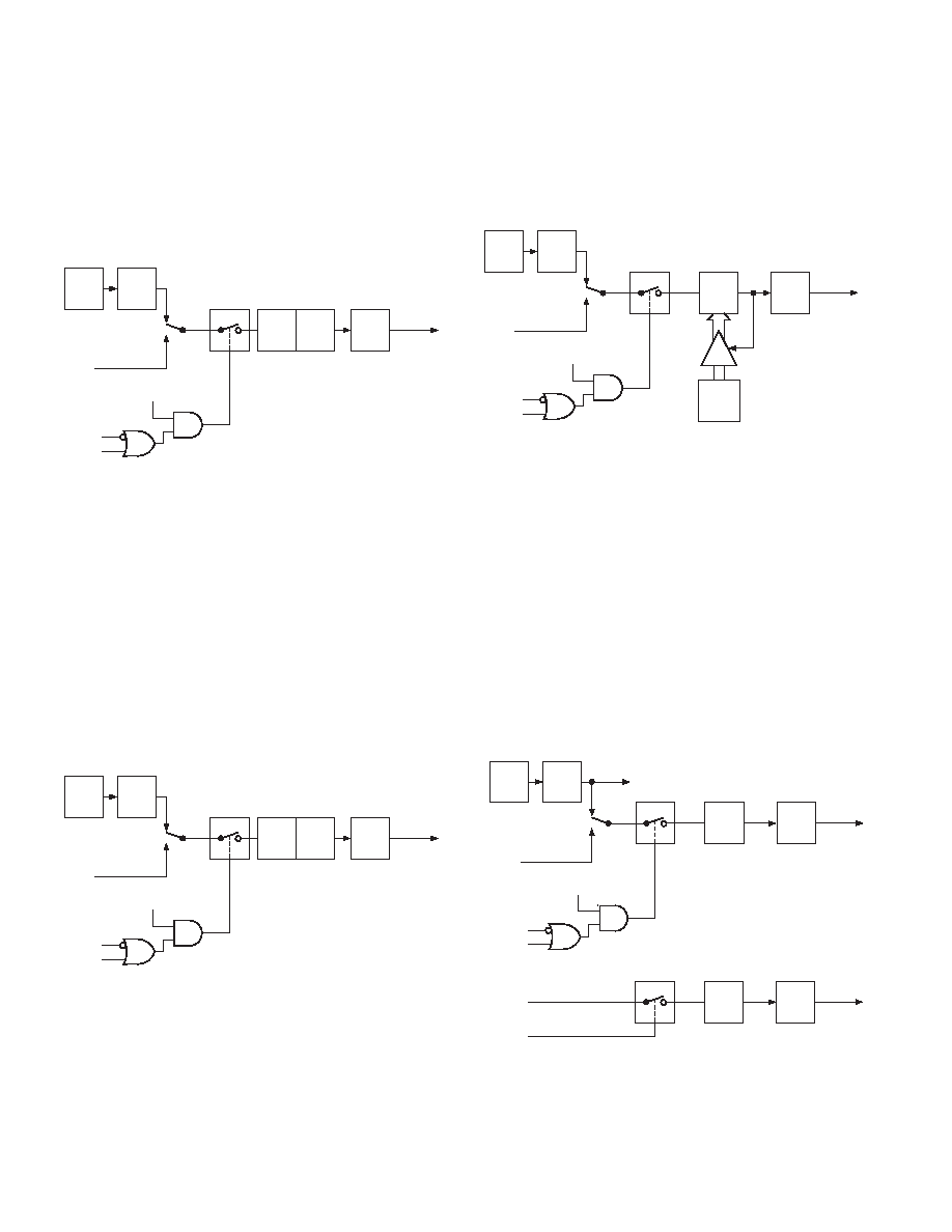
Mode 0 (13-Bit Timer/Counter)
Mode 0 configures an 8-bit timer/counter with a divide-by-32
prescaler. Figure 48 shows Mode 0 operation.
12
CORE
CLK*
CONTROL
P3.4/T0
GATE
P3.2/
INT0
TR0
TF0
TL0
(5 BITS)
TH0
(8 BITS)
INTERRUPT
C/
T = 0
C/
T = 1
*THE CORE CLOCK IS THE OUTPUT OF THE PLL (SEE "ON-CHIP PLL")
Figure 48. Timer/Counter 0, Mode 0
In this mode, the timer register is configured as a 13-bit register.
As the count rolls over from all 1s to all 0s, it sets the timer over-
flow flag. The overflow flag, TF0, can then be used to request
an interrupt. The counted input is enabled to the timer when
TR0 = 1 and either Gate = 0 or
INT0 = 1. Setting Gate = 1 allows
the timer to be controlled by external input
INT0, to facilitate
pulsewidth measurements. TR0 is a control bit in the special
function register TCON; Gate is in TMOD. The 13-bit register
consists of all eight bits of TH0 and the lower five bits of TL0.
The upper three bits of TL0 are indeterminate and should be
ignored. Setting the run flag (TR0) does not clear the registers.
Mode 1 (16-Bit Timer/Counter)
Mode 1 is the same as Mode 0, except that the timer register is
running with all 16 bits. Mode 1 is shown in Figure 49.
12
CORE
CLK*
CONTROL
P3.4/T0
GATE
P3.2/
INT0
TR0
TF0
TL0
(8 BITS)
TH0
(8 BITS)
INTERRUPT
C/
T = 0
C/
T = 1
*THE CORE CLOCK IS THE OUTPUT OF THE PLL (SEE "ON-CHIP PLL")
Figure 49. Timer/Counter 0, Mode 1
Mode 2 (8-Bit Timer/Counter with Auto Reload)
Mode 2 configures the timer register as an 8-bit counter (TL0)
with automatic reload, as shown in Figure 50. Overflow from
TL0 not only sets TF0, but also reloads TL0 with the contents
of TH0, which are preset by software. The reload leaves TH0
unchanged.
CONTROL
TF0
TL0
(8 BITS)
INTERRUPT
RELOAD
TH0
(8 BITS)
12
CORE
CLK*
P3.4/T0
GATE
P3.2/
INT0
TR0
C/
T = 0
C/
T = 1
*THE CORE CLOCK IS THE OUTPUT OF THE PLL (SEE "ON-CHIP PLL")
Figure 50. Timer/Counter 0, Mode 2
Mode 3 (Two 8-Bit Timer/Counters)
Mode 3 has different effects on Timer 0 and Timer 1. Timer 1 in
Mode 3 simply holds its count. The effect is the same as setting
TR1 = 0. Timer 0 in Mode 3 establishes TL0 and TH0 as two
separate counters. This configuration is shown in Figure 51.
TL0 uses the timer 0 control bits: C/
T, Gate, TR0, INT0, and
TF0. TH0 is locked into a timer function (counting machine
cycles) and takes over the use of TR1 and TF1 from Timer 1.
Thus, TH0 now controls the “Timer 1” interrupt. Mode 3 is
provided for applications requiring an extra 8-bit timer or counter.
When Timer 0 is in Mode 3, Timer 1 can be turned on and off
by switching it out of and into its own Mode 3, or can still be
used by the serial interface as a baud rate generator. In fact, it
can be used, in any application not requiring an interrupt from
Timer 1 itself.
CONTROL
TF0
TL0
(8 BITS)
INTERRUPT
12
CORE
CLK*
P3.4/T0
GATE
P3.2/
INT0
TR0
C/
T = 0
C/
T = 1
*THE CORE CLOCK IS THE OUTPUT OF THE PLL (SEE "ON-CHIP PLL")
CORE
CLK/12
TF1
TH0
(8 BITS)
INTERRUPT
CORE
CLK/12
TR1
Figure 51. Timer/Counter 0, Mode 3
相关PDF资料 |
PDF描述 |
|---|---|
| VI-JVP-IY-F2 | CONVERTER MOD DC/DC 13.8V 50W |
| VE-B3D-IY-F2 | CONVERTER MOD DC/DC 85V 50W |
| AT91SAM9XE256-QU | MCU ARM9 256K FLASH 208-PQFP |
| VI-JVN-IY-F4 | CONVERTER MOD DC/DC 18.5V 50W |
| VI-JVM-IY-F2 | CONVERTER MOD DC/DC 10V 50W |
相关代理商/技术参数 |
参数描述 |
|---|---|
| ADUC836 | 制造商:AD 制造商全称:Analog Devices 功能描述:MicroConverter, Dual 16-Bit-ADCs with Embedded 62 kB Flash MCU |
| ADUC836_02 | 制造商:AD 制造商全称:Analog Devices 功能描述:MicroConverter, Dual 16-Bit ADCs with Embedded 62 kB Flash MCU |
| ADUC836BCP | 制造商:Rochester Electronics LLC 功能描述: 制造商:Analog Devices 功能描述: |
| ADUC836BCPZ | 功能描述:IC MCU 62K FLASH ADC/DAC 56LFCSP RoHS:是 类别:集成电路 (IC) >> 嵌入式 - 微控制器, 系列:MicroConverter® ADuC8xx 标准包装:38 系列:Encore!® XP® 核心处理器:eZ8 芯体尺寸:8-位 速度:5MHz 连通性:IrDA,UART/USART 外围设备:欠压检测/复位,LED,POR,PWM,WDT 输入/输出数:16 程序存储器容量:4KB(4K x 8) 程序存储器类型:闪存 EEPROM 大小:- RAM 容量:1K x 8 电压 - 电源 (Vcc/Vdd):2.7 V ~ 3.6 V 数据转换器:- 振荡器型:内部 工作温度:-40°C ~ 105°C 封装/外壳:20-SOIC(0.295",7.50mm 宽) 包装:管件 其它名称:269-4116Z8F0413SH005EG-ND |
| ADUC836BCPZ-REEL | 功能描述:IC MCU 62K FLASH ADC/DAC 56LFCSP RoHS:是 类别:集成电路 (IC) >> 嵌入式 - 微控制器, 系列:MicroConverter® ADuC8xx 标准包装:38 系列:Encore!® XP® 核心处理器:eZ8 芯体尺寸:8-位 速度:5MHz 连通性:IrDA,UART/USART 外围设备:欠压检测/复位,LED,POR,PWM,WDT 输入/输出数:16 程序存储器容量:4KB(4K x 8) 程序存储器类型:闪存 EEPROM 大小:- RAM 容量:1K x 8 电压 - 电源 (Vcc/Vdd):2.7 V ~ 3.6 V 数据转换器:- 振荡器型:内部 工作温度:-40°C ~ 105°C 封装/外壳:20-SOIC(0.295",7.50mm 宽) 包装:管件 其它名称:269-4116Z8F0413SH005EG-ND |
发布紧急采购,3分钟左右您将得到回复。