- 您现在的位置:买卖IC网 > PDF目录166397 > B900J24PXX12I 0-BIT, 80 MHz, OTHER DSP, PQFP44 PDF资料下载
参数资料
| 型号: | B900J24PXX12I |
| 元件分类: | 数字信号处理 |
| 英文描述: | 0-BIT, 80 MHz, OTHER DSP, PQFP44 |
| 文件页数: | 4/100页 |
| 文件大小: | 1547K |
| 代理商: | B900J24PXX12I |
第1页第2页第3页当前第4页第5页第6页第7页第8页第9页第10页第11页第12页第13页第14页第15页第16页第17页第18页第19页第20页第21页第22页第23页第24页第25页第26页第27页第28页第29页第30页第31页第32页第33页第34页第35页第36页第37页第38页第39页第40页第41页第42页第43页第44页第45页第46页第47页第48页第49页第50页第51页第52页第53页第54页第55页第56页第57页第58页第59页第60页第61页第62页第63页第64页第65页第66页第67页第68页第69页第70页第71页第72页第73页第74页第75页第76页第77页第78页第79页第80页第81页第82页第83页第84页第85页第86页第87页第88页第89页第90页第91页第92页第93页第94页第95页第96页第97页第98页第99页第100页
Advance Data Sheet
B900
July 1999
Baseband Signal Processor
Lucent Technologies Inc.
11
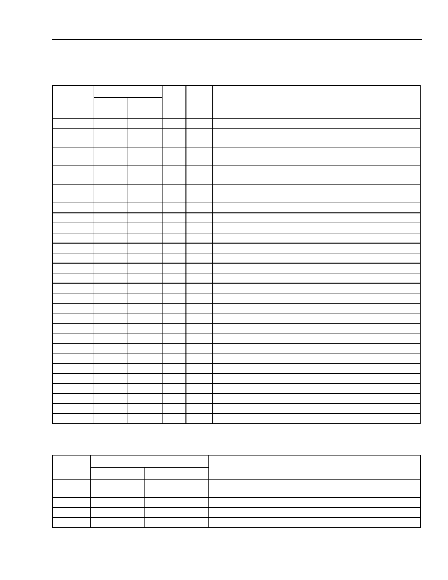
3 Pin Information (continued)
Table 2. B900 Power Supply, Ground, and Unconnected Pins
Table 1. B900 Pinout
Symbol
Pin Number
Type
Active
Pin Description
44-Pin
PLCC
44-Pin
MQFP
DOUT
42
36
O
High
Processor clock; digital output/clock output.
INTB*
* Multiplexed with IOP pins.
11
5
I
Neg
External interrupt, negative edge-triggered; multiplexed with
IOPB0.
IOPA[7:0]
12—17,
20—21
6—11,
14—15
I/O
Pgm
I/O port A (bits 7—0).
IOPB[7:0]
2—5,
8—11
40—43,
2—5
I/O
Pgm
I/O port B (bits 7—0).
IOPC[7:0]
22—27,
30—31
16—21,
24—25
I/O
Pgm
I/O port C (bits 7—0).
IOPD[3:0]
32—35
26—29
I/O
Pgm
I/O port D (bits 3—0).
JTSEL*
8
2
I
High
JTAG select. (JTSEL is multiplexed with IOPB3.)
MDISDO*
22
16
I/O
—
SSI master data in/slave data out; multiplexed with IOPC7.
MDOSDI*
23
17
I/O
—
SSI master data out/slave data in; multiplexed with IOPC6.
10
4
I
High
Oscillator bypass. (OSCBYP is multiplexed with IOPB1.)
RSTB
43
37
I/O
Low
Reset.
SCK*
24
18
I/O
—
SSI serial clock; multiplexed with IOPC5.
SSN*
25
19
I
Low
SSI serial slave select; multiplexed with IOPC4.
TCK*
30
24
I
—
Test clock (JTAG). (TCK is multiplexed with IOPC1.)
TDI*
27
21
I
High
Test data in (JTAG). (TDI is multiplexed with IOPC2.)
26
20
O
High
Test data out (JTAG). (TDO is multiplexed with IOPC3.)
31
25
I
High
Test mode select (JTAG). (TMS is multiplexed with IOPC0.)
CASN*
35
29
O
Low
Column address select. (CASN is multiplexed with IOPD0.)
RASN*
34
28
O
Low
Row address select. (RASN is multiplexed with IOPD1.)
RWN*
33
27
O
High
Read/write not. (RWN is multiplexed with IOPD2.)
XTALA
38
32
I
—
Crystal oscillator connection.
XTALB
37
31
I/O
—
Crystal oscillator connection.
SDI*
2
40
I
—
SIO data in; multiplexed with IOPB7.
3
41
O
—
SIO data out; multiplexed with IOPB6.
4
42
I/O
—
SIO shift clock; multiplexed with IOPB5.
SLDA*
5
43
I/O
—
SIO channel A load clock; multiplexed with IOPB4.
9
3
I/O
—
SIO channel B load clock; multiplexed with IOPB2.
Symbol
Pin Number
Type
44-Pin PLCC
44-Pin MQFP
VDD
7, 19, 29, 41,
44
1, 13, 23, 35, 38
The B900 can support both 5 V and 3 V.
VSS
1, 6, 18, 28, 36
12, 22, 30, 39, 44 Ground for digital circuitry.
VDDA
40
34
Supply for phase-locked loop (should be connected to VDD).
VSSA
39
33
Ground for phase-locked loop (should be connected to VSS).
相关PDF资料 |
PDF描述 |
|---|---|
| B900J24FXX12IT | 0-BIT, 59.88 MHz, OTHER DSP, PQFP44 |
| BA00CC0WCP-V5 | 1A Low Dropout Voltage Regulator with Shut Down Switch(Adustable Voltage) |
| BA10E6 | COPPER ALLOY, TIN FINISH, RING TERMINAL |
| BA12004 | 0.5 A, 7 CHANNEL, NPN, Si, POWER TRANSISTOR |
| BA1518SUR5VP | SINGLE COLOR DISPLAY CLUSTER, ULTRA RED |
相关代理商/技术参数 |
参数描述 |
|---|---|
| B-900-M-10 | 制造商:Thomas & Betts 功能描述: |
| B-900-M-10-EG | 制造商:Thomas & Betts 功能描述: |
| B-900-M-20 | 制造商:Thomas & Betts 功能描述: |
| B-900-M-20-EG | 制造商:Thomas & Betts 功能描述: |
| B901 | 制造商:EDAL 制造商全称:EDAL 功能描述:Silicon Bridge Rectifier |
发布紧急采购,3分钟左右您将得到回复。