- 您现在的位置:买卖IC网 > PDF目录1924 > IDT82P2828BHG (IDT, Integrated Device Technology Inc)IC LIU T1/J1/E1 28+1CH 640-PBGA PDF资料下载
参数资料
| 型号: | IDT82P2828BHG |
| 厂商: | IDT, Integrated Device Technology Inc |
| 文件页数: | 82/154页 |
| 文件大小: | 0K |
| 描述: | IC LIU T1/J1/E1 28+1CH 640-PBGA |
| 标准包装: | 5 |
| 类型: | 线路接口装置(LIU) |
| 规程: | E1 |
| 电源电压: | 3.13 V ~ 3.47 V |
| 安装类型: | 表面贴装 |
| 封装/外壳: | 640-BGA 裸露焊盘 |
| 供应商设备封装: | 640-PBGA-EP(31x31) |
| 包装: | 托盘 |
| 其它名称: | 82P2828BHG |
第1页第2页第3页第4页第5页第6页第7页第8页第9页第10页第11页第12页第13页第14页第15页第16页第17页第18页第19页第20页第21页第22页第23页第24页第25页第26页第27页第28页第29页第30页第31页第32页第33页第34页第35页第36页第37页第38页第39页第40页第41页第42页第43页第44页第45页第46页第47页第48页第49页第50页第51页第52页第53页第54页第55页第56页第57页第58页第59页第60页第61页第62页第63页第64页第65页第66页第67页第68页第69页第70页第71页第72页第73页第74页第75页第76页第77页第78页第79页第80页第81页当前第82页第83页第84页第85页第86页第87页第88页第89页第90页第91页第92页第93页第94页第95页第96页第97页第98页第99页第100页第101页第102页第103页第104页第105页第106页第107页第108页第109页第110页第111页第112页第113页第114页第115页第116页第117页第118页第119页第120页第121页第122页第123页第124页第125页第126页第127页第128页第129页第130页第131页第132页第133页第134页第135页第136页第137页第138页第139页第140页第141页第142页第143页第144页第145页第146页第147页第148页第149页第150页第151页第152页第153页第154页
IDT82P2828
28(+1) CHANNEL HIGH-DENSITY T1/E1/J1 LINE INTERFACE UNIT
Functional Description
33
February 6, 2009
3.2.3
SLICER
The Slicer is used to generate a standard amplitude mark or a space
according to the amplitude of the input signals. The input signal is sliced
at 50% of the peak value.
3.2.4
RX CLOCK & DATA RECOVERY
The Rx Clock & Data Recovery is used to recover the clock signal
from the received data. It is accomplished by an integrated Digital Phase
Locked Loop (DPLL). The recovered clock tracks the jitter in the data
output from the Slicer and keeps the phase relationship between data
and clock during the absence of the incoming pulse.
Note that the IDT82P2828 also provides programmable REFA and
REFB pins to output any of the 29 recovered line clocks. Refer to
Section 3.6 Clock Inputs and Outputs for details.
3.2.5
DECODER
The Decoder is used only when the receive system interface is in
Single Rail NRZ Format mode. When the receive system interface is in
other modes, the Decoder is bypassed automatically. (Refer to
Section 3.2.6 Receive System Interface for the description of the receive
system interface).
In T1/J1 mode, the received signal is decoded by AMI or B8ZS line
code rule. In E1 mode, the received signal is decoded by AMI or HDB3
line code rule. The line code rule is selected by the R_CODE bit (b2,
3.2.6
RECEIVE SYSTEM INTERFACE
The received data can be output to the system side in four modes:
Single Rail NRZ Format mode, Dual Rail NRZ Format mode, Dual Rail
RZ Format mode and Dual Rail Sliced mode, as selected by the
R_MD[1:0] bits (b1~0, RCF1).
If data is output on RDn in NRZ format and the recovered clock is
output on RCLKn, the receive system interface is in Single Rail NRZ
Format mode. In this mode, the data is decoded and updated on the
active edge of RCLKn. RCLKn outputs a 1.544 MHz (in T1/J1 mode) or
2.048 MHz (in E1 mode) clock. The Receive Multiplex Function (RMFn)
signal is updated on the active edge of RCLKn and can be selected to
indicate PRBS/ARB, LAIS, LEXZ, LBPV, LEXZ + LBPV, LLOS, output
recovered clock (RCLK) or XOR output of positive and negative sliced
data. Refer to Section 3.5.7.1 RMFn Indication for the description of
RMFn.
If data is output on RDPn and RDNn in NRZ format and the recov-
ered clock is output on RCLKn, the receive system interface is in Dual
Rail NRZ Format mode. In this mode, the data is un-decoded and
updated on the active edge of RCLKn. RCLKn outputs a 1.544 MHz (in
T1/J1 mode) or 2.048 MHz (in E1 mode) clock.
If data is output on RDPn and RDNn in RZ format and the recovered
clock is output on RCLKn, the receive system interface is in Dual Rail
RZ Format mode. In this mode, the data is un-decoded and updated on
the active edge of RCLKn. RCLKn outputs a 1.544 MHz (in T1/J1 mode)
or 2.048 MHz (in E1 mode) clock.
If data is output on RDPn and RDNn in RZ format directly after
passing through the Slicer, the receive system interface is in Dual Rail
Sliced mode. In this mode, the data is raw sliced and un-decoded.
RMFn can be selected to indicate PRBS/ARB, LAIS, LEXZ, LBPV, LEXZ
+ LBPV, LLOS, output recovered clock (RCLK) or XOR output of positive
and negative sliced data. Refer to Chapter 3.5.7.1 RMFn Indication for
the description of RMFn.
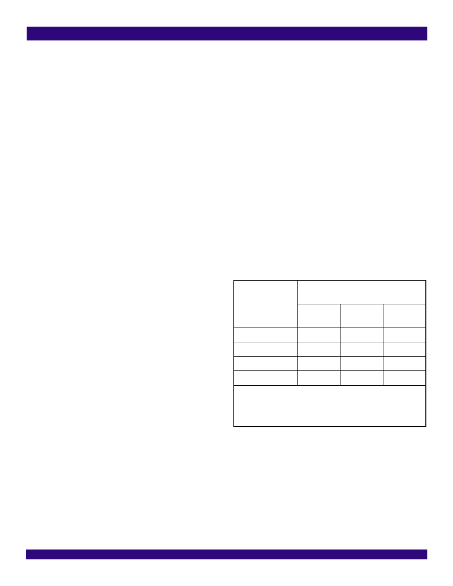
Table-3 summarizes the multiplex pin used in different receive
system interface.
Table-3 Multiplex Pin Used in Receive System Interface
Receive System
Interface
Multiplex Pin Used On Receive System
Interface
RDn / RDPn
RDNn / RMFn
RCLKn /
RMFn
Single Rail NRZ Format
RDn 1
RMFn 2
RCLKn 3
Dual Rail NRZ Format
RDPn 1
RDNn 1
RCLKn 3
Dual Rail RZ Format
RDPn 1
RDNn 1
RCLKn 3
Dual Rail Sliced
RDPn 1
RDNn 1
RMFn 2
Note:
1. The active level on RDn, RDPn and RDNn is selected by the RD_INV bit (b3,
RCF1,...).
2. RMFn is always active high.
3. The active edge of RCLKn is selected by the RCK_ES bit (b4, RCF1,...).
相关PDF资料 |
PDF描述 |
|---|---|
| IDT82P2916BFG | IC LIU T1/E1/J1 16CH SH 484BGA |
| IDT82P5088BBG | IC LIU T1/E1/J1 OCTAL 256PBGA |
| IDT82V2041EPPG | IC LIU T1/J1/E1 1CH 44-TQFP |
| IDT82V2042EPFG | IC LIU T1/J1/E1 2CH SHORT 80TQFP |
| IDT82V2044EPFG | IC LIU T1/E1 QUAD SHORT 128-TQFP |
相关代理商/技术参数 |
参数描述 |
|---|---|
| IDT82P2916 | 制造商:IDT 制造商全称:Integrated Device Technology 功能描述:16-Channel High-Density T1/E1/J1 Line Interface Unit |
| IDT82P2916BFG | 功能描述:IC LIU T1/E1/J1 16CH SH 484BGA RoHS:是 类别:集成电路 (IC) >> 接口 - 电信 系列:- 产品培训模块:Lead (SnPb) Finish for COTS 产品变化通告:Product Discontinuation 06/Feb/2012 标准包装:750 系列:* |
| IDT82P2916BFG8 | 制造商:Integrated Device Technology Inc 功能描述:IC LIU T1/E1/J1 16CH SH 484BGA |
| IDT82P5088 | 制造商:IDT 制造商全称:Integrated Device Technology 功能描述:Universal Octal T1/E1/J1 LIU with Integrated Clock Adapter |
| IDT82P5088BBBLANK | 制造商:IDT 制造商全称:Integrated Device Technology 功能描述:Universal Octal T1/E1/J1 LIU with Integrated Clock Adapter |
发布紧急采购,3分钟左右您将得到回复。