- 您现在的位置:买卖IC网 > PDF目录1924 > IDT88P8341BHI (IDT, Integrated Device Technology Inc)IC SPI3-SPI4 EXCHANGE 820-PBGA PDF资料下载
参数资料
| 型号: | IDT88P8341BHI |
| 厂商: | IDT, Integrated Device Technology Inc |
| 文件页数: | 72/96页 |
| 文件大小: | 0K |
| 描述: | IC SPI3-SPI4 EXCHANGE 820-PBGA |
| 标准包装: | 24 |
| 系列: | * |
| 其它名称: | 88P8341BHI |
第1页第2页第3页第4页第5页第6页第7页第8页第9页第10页第11页第12页第13页第14页第15页第16页第17页第18页第19页第20页第21页第22页第23页第24页第25页第26页第27页第28页第29页第30页第31页第32页第33页第34页第35页第36页第37页第38页第39页第40页第41页第42页第43页第44页第45页第46页第47页第48页第49页第50页第51页第52页第53页第54页第55页第56页第57页第58页第59页第60页第61页第62页第63页第64页第65页第66页第67页第68页第69页第70页第71页当前第72页第73页第74页第75页第76页第77页第78页第79页第80页第81页第82页第83页第84页第85页第86页第87页第88页第89页第90页第91页第92页第93页第94页第95页第96页
74
IDT88P8341 SPI EXCHANGE SPI-3 TO SPI-4
INDUSTRIALTEMPERATURERANGE
APRIL 10, 2006
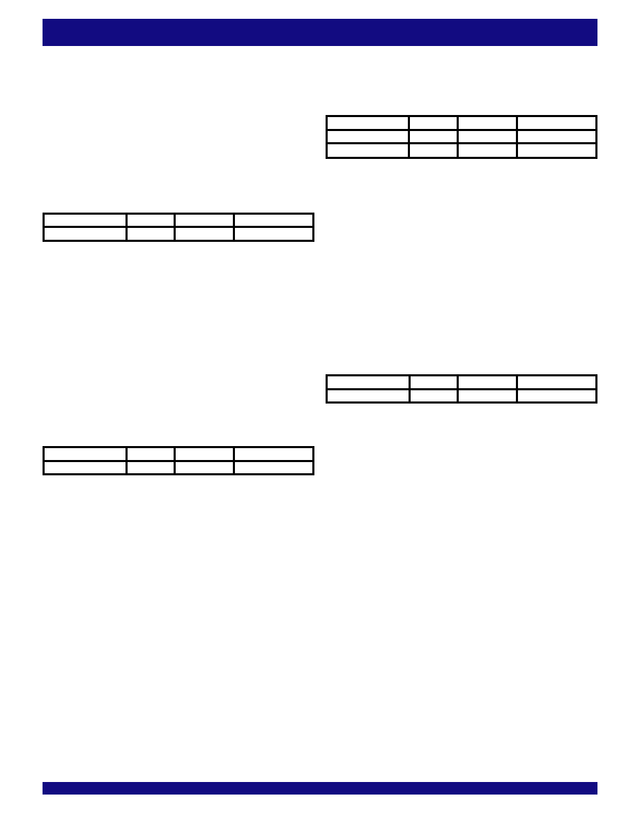
TABLE 115 - SPI-4 EGRESS CONTROL LANE
TIMING REGISTER (REGISTER_OFFSET 0x2B)
Field
Bits
Length
Initial Value
CTLTC[1:0]
1:0
2
0
TABLE 116 - SPI-4 EGRESS DATA CLOCK TIMING
REGISTER(REGISTER_OFFSET0x2C)
Field
Bits
Length
Initial Value
DCTC[3:0]
3:0
4
0
TABLE 117 - SPI-4 EGRESS STATUS TIMING
REGISTER (REGISTER_OFFSET 0x2D)
Field
Bits
Length
Initial Value
STC0[1:0]
1:0
2
0
STC1[1:0]
3:2
2
0
TABLE 118 - SPI-4 EGRESS STATUS CLOCK TIM-
ING REGISTER (REGISTER_OFFSET 0x2E)
Field
Bits
Length
Initial Value
SCTC[3:0]
3:0
4
0
DTCn [1:0]
Used for adding 0.1 clock cycles of output delay to SPI-
4 egress data lane n.
[1:0]=0=No added delay
[1:0]=1=Add 0.1 clock cycle of delay to data lane n
[1:0]=2=Add 0.2 clock cycles of delay to data lane n
[1:0]=3=Add 0.3 clock cycles of delay to data lane n
SPI-4 egress control lane timing register
(Block_base 0x0800 + Register_offset 0x2B)
SPI-4 egress status timing register (Block_base
0x0800 + Register_offset 0x2D)
TheSPI-4egresscontrol lanetimingregisteratBlock_base0x0800hasread
and write access. The SPI-4 egress controllane timing register is used to
manually align the phase of the control lane by adding from 0.1 clock cycle to
0.3 clock cycles of delay.
CTLTC [1:0]
Usedforadding0.1clockcycles ofoutputdelaytotheSPI-
4 egress control output.
[1:0]=0=No added delay
[1:0]=1=Add 0.1 clock cycle of delay to the control output
[1:0]=2=Add 0.2 clock cycles of delay to the control output
[1:0]=3=Add 0.3 clock cycles of delay to the control output
SPI-4 egress data clock timing register
(Block_base 0x0800 + Register_offset 0x2C)
The SPI-4 egress data clock timing control register at Block_base 0x0800
has read and write access. The SPI-4 egress data clock timing control register
is used to manually align the phase of the SPI-4 egress data clock to the data
and control lanes by adding from 0.1 clock cycle to 0.9 clock cycles of delay to
thedataclock.Notethattapselectionisnotmonotonicwiththenumberinbitfield
[3:0].
DCTC [3:0]
Used for adding 0.1clock cycles of output delay to the SPI-
4 egress data clock.
[3:0]=0=No added delay
[3:0]=1=Add 0.1 clock cycle of delay to the SPI-4 egress data clock
[3:0]=3=Add 0.2 clock cycles of delay to the SPI-4 egress data clock
[3:0]=2=Add 0.3 clock cycles of delay to the SPI-4 egress data clock
[3:0]=7=Add 0.4 clock cycles of delay to the SPI-4 egress data clock
[3:0]=6=Add 0.5 clock cycles of delay to the SPI-4 egress data clock
[3:0]=4=Add 0.6 clock cycles of delay to the SPI-4 egress data clock
[3:0]=5=Add 0.7 clock cycles of delay to the SPI-4 egress data clock
[3:0]=F=Add0.8clock cyclesof delay to the SPI-4 egressdataclock
[3:0]=E=Add0.9clockcyclesofdelaytotheSPI-4egressdataclock
TheSPI-4egressstatustimingregisteratBlock_base0x0800+Register_offset
0x2Dhasreadandwriteaccess.TheSPI-4egressstatustiming registerisused
to manually align the phase of the status lane n by adding from 0.1 clock cycle
to 0.3 clock cycles of delay. The STC0[1:0] and STC1[1:0] fields are valid only
for LVDS status, not for LVTTL status.
STCn [1:0]
Used for adding 0.1 clock cycles of output delay to SPI-
4 egress status lane n.
[1:0]=0=No added delay
[1:0]=1=Add 0.1 clock cycle of delay to status lane n
[1:0]=2=Add 0.2 clock cycles of delay to status lane n
[1:0]=3=Add 0.3 clock cycles of delay to status lane n
SPI-4 egress status clock timing register
(Block_base 0x0800 + Register_offset 0x2E)
The SPI-4 egress status clock timing register at Block_base 0x0800 +
Register_offset0x2Ehasreadandwriteaccess.TheSPI-4egressstatusclock
timingregisterisusedtomanuallyalignthephaseoftheSPI-4egressstatusclock
to the status outputs by adding from 0.1 clock cycle to 0.9 clock cycles of delay
tothestatusclockoutput.Notethattapselectionisnotmonotonicwiththenumber
in bit field [3:0].
SCTC [3:0]
Usedforadding0.1clockcyclesofoutputdelaytotheSPI-
4 egress status clock output.
[3:0]=0=No added delay
[3:0]=1=Add0.1clockcycleofdelaytotheSPI-4egressstatusclock
[3:0]=3=Add0.2clockcyclesofdelaytotheSPI-4egressstatusclock
[3:0]=2=Add0.3clockcyclesofdelaytotheSPI-4egressstatusclock
[3:0]=7=Add0.4clockcyclesofdelaytotheSPI-4egressstatusclock
[3:0]=6=Add0.5clockcyclesofdelaytotheSPI-4egressstatusclock
[3:0]=4=Add0.6clockcyclesofdelaytotheSPI-4egressstatusclock
[3:0]=5=Add0.7clockcyclesofdelaytotheSPI-4egressstatusclock
[3:0]=F=Add0.8clockcyclesofdelaytotheSPI-4egressstatusclock
[3:0]=E=Add0.9clockcyclesofdelaytotheSPI-4egressstatusclock
相关PDF资料 |
PDF描述 |
|---|---|
| IDT88P8342BHI | IC SPI3-SPI4 EXCHANGE 820-PBGA |
| IDT88P8344BHI | IC SPI3-SPI4 EXCHANGE 820-PBGA |
| IDT89H24NT24G2ZBHLG | IC PCI SW 24LANE 24PORT 324BGA |
| IDT89HPES16NT2ZBBCG | IC PCI SW 16LANE 2PORT 484-CABGA |
| IDT89HPES24NT3ZBBXG | IC PCI SW 24LANE 3PORT 420-SBGA |
相关代理商/技术参数 |
参数描述 |
|---|---|
| IDT88P8342BHGI | 功能描述:IC SPI3-SPI4 EXCHANGE 820-PBGA RoHS:是 类别:集成电路 (IC) >> 专用 IC 系列:* 产品培训模块:Lead (SnPb) Finish for COTS Obsolescence Mitigation Program 标准包装:1 系列:- 类型:调帧器 应用:数据传输 安装类型:表面贴装 封装/外壳:400-BBGA 供应商设备封装:400-PBGA(27x27) 包装:散装 |
| IDT88P8342BHI | 功能描述:IC SPI3-SPI4 EXCHANGE 820-PBGA RoHS:否 类别:集成电路 (IC) >> 专用 IC 系列:* 产品培训模块:Lead (SnPb) Finish for COTS Obsolescence Mitigation Program 标准包装:1 系列:- 类型:调帧器 应用:数据传输 安装类型:表面贴装 封装/外壳:400-BBGA 供应商设备封装:400-PBGA(27x27) 包装:散装 |
| IDT88P8344 | 制造商:IDT 制造商全称:Integrated Device Technology 功能描述:SPI EXCHANGE 4 x SPI-3 TO SPI-4 Issue 1.0 |
| IDT88P8344BHGI | 功能描述:IC SPI3-SPI4 EXCHANGE 820-PBGA RoHS:是 类别:集成电路 (IC) >> 专用 IC 系列:* 产品培训模块:Lead (SnPb) Finish for COTS Obsolescence Mitigation Program 标准包装:1 系列:- 类型:调帧器 应用:数据传输 安装类型:表面贴装 封装/外壳:400-BBGA 供应商设备封装:400-PBGA(27x27) 包装:散装 |
| IDT88P8344BHI | 功能描述:IC SPI3-SPI4 EXCHANGE 820-PBGA RoHS:否 类别:集成电路 (IC) >> 专用 IC 系列:* 产品培训模块:Lead (SnPb) Finish for COTS Obsolescence Mitigation Program 标准包装:1 系列:- 类型:调帧器 应用:数据传输 安装类型:表面贴装 封装/外壳:400-BBGA 供应商设备封装:400-PBGA(27x27) 包装:散装 |
发布紧急采购,3分钟左右您将得到回复。