- 您现在的位置:买卖IC网 > PDF目录4578 > IDT88P8344BHGI (IDT, Integrated Device Technology Inc)IC SPI3-SPI4 EXCHANGE 820-PBGA PDF资料下载
参数资料
| 型号: | IDT88P8344BHGI |
| 厂商: | IDT, Integrated Device Technology Inc |
| 文件页数: | 36/98页 |
| 文件大小: | 0K |
| 描述: | IC SPI3-SPI4 EXCHANGE 820-PBGA |
| 标准包装: | 24 |
| 系列: | * |
| 其它名称: | 88P8344BHGI |
第1页第2页第3页第4页第5页第6页第7页第8页第9页第10页第11页第12页第13页第14页第15页第16页第17页第18页第19页第20页第21页第22页第23页第24页第25页第26页第27页第28页第29页第30页第31页第32页第33页第34页第35页当前第36页第37页第38页第39页第40页第41页第42页第43页第44页第45页第46页第47页第48页第49页第50页第51页第52页第53页第54页第55页第56页第57页第58页第59页第60页第61页第62页第63页第64页第65页第66页第67页第68页第69页第70页第71页第72页第73页第74页第75页第76页第77页第78页第79页第80页第81页第82页第83页第84页第85页第86页第87页第88页第89页第90页第91页第92页第93页第94页第95页第96页第97页第98页
41
IDT88P8344 SPI EXCHANGE 4 x SPI-3 TO SPI-4
INDUSTRIALTEMPERATURERANGE
APRIL 10, 2006
8. OPERATION GUIDE
8.1 Hardware operation
8.1.1 System reset
There are two methods for resetting the device: hardware reset & software
reset. During reset the output clocks are not toggled.
Hardware reset
The RESETB input requires an active low pulse to reset the internal logic.
Software reset
The software reset is triggered by setting to 1 the SW_RESET field in direct
register Software Reset Register (p.51). The response to a software reset is
identical to a hardware rest except that software reset does not change the
N_OCLK[3:0] fields in the Clock Generator Control Register (p.77), so it does
not impact the clock generators. The SW_RESET field is self-clear to 0 after the
device initialized itself.After software reset the external microprocessor should
have delay of at least 1ms before accessing the device, and then.After the 1ms
delay, the user should poll the INIT_DONE field in the Software Reset Register
(p.51), and wait till it is 1. When the INIT_DONE field is 1, the user should
download a boot code from the external microprocessor flash to the device
embedded processor RAM.
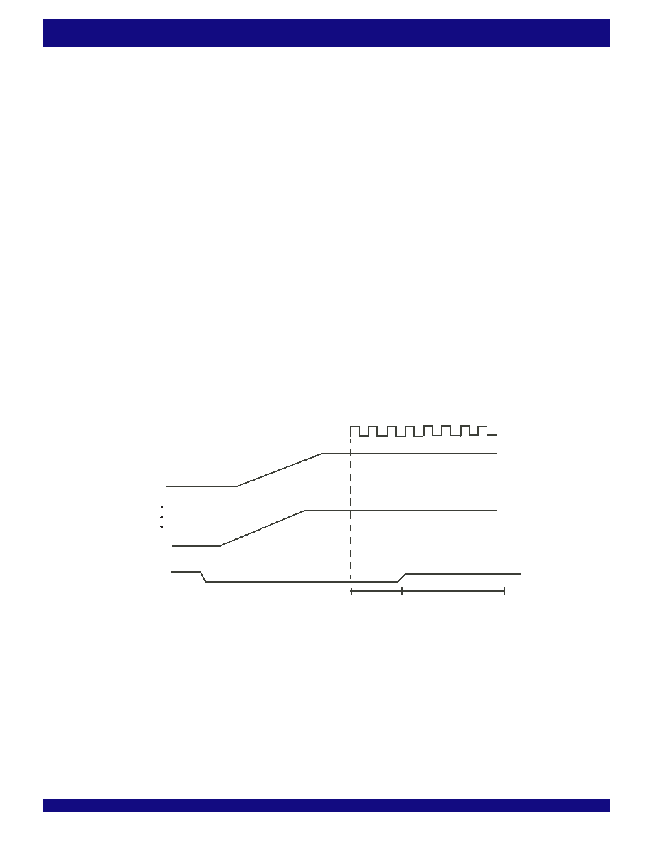
8.1.2 Power on sequence
A correct power-on-reset sequence is crucial for the normal behavior of
the device. The power-on-reset sequence includes the following signals:
CLK (REF_CLK or I_DCLK - depends on which of theses pins are selected),
VDDT33, VDDC12 and RESETB. Figure 32, Power-on-Reset Sequence
illustrates the recommended implementation for the power-on-reset sequence
for the device. IDT recommends powering up the VDD33 power supply first,
and the VDDC18 power supply last. The power supplies can be also powered
up in the same time. There is no requirement for the minimum or maximum
delay between the power-up of the power supplies. The power supplies
should be powered off in the revers order. The power ramp should not be fast
than 100us, but also not too slow.
When the power supplies are powered up, the RESETB signal should be
at low level. During power-on-reset, after the VDDT33, VDDC18, CLK
(REF_CLK or I_DCLK - depends on which of theses pins are selected) and
the configuration signals are stable, the RESETB signal should remain at a low
level at least 10ms (symbol “T1”) to reset the internal logic. After the RESETB
pulse ends, the device starts generating the SPI-4 / SPI-3 external output
clocks & the MCLK internal clock.
After the RESETB pulse ends, a delay of 1ms should be added (symbols
“T2”) before accessing the device for initialization and configuration. This
allows the internal logic to be stable. During T2 (at least 1ms delay) the device
performs internal memories initialization.
After T2, the user should poll the INIT_DONE field in the in the Software
Reset Register (p.51), and wait till it is 1. When the INIT_DONE field is 1, the
user should download a boot code from the external microprocessor flash to
the device embedded processor RAM.
T1
CLK
VDDT33
RESETB
T2
VDDC18
6370 drw23a
8.1.3 Clock domains
The chip has several clock domains. The related registers can not be
configured without each clock. It is necessary to supply the clocks that are
pertinenttotheregistersbeinginitializedfortheinitializationtosucceed.Inorder
toaccessthemicroprocessorinterface,MCLKmustbeactive,eitherbyselecting
andprovidingastableREF_CLKinput,orbyselectingandensuringthatastable
clock is always present on the I_DCLK input. The selection of either the
REF_CLK or the I_DCLK clock inputs is described in Table 14 CK_SEL[3:0]
input pin decoding.
8.2 Software operation
8.2.1 Chip configuration sequence
Forproperdeviceoperation,itisimportanttoinitializetheIDT88P8344inthe
correct sequence following reset. This sequence is outlined in the following
paragraphs.
1) Reset the IDT88P8344 chip. After reset, the chip will perform auto
initialization.Waitforthechipinitializationtocomplete.TheINIT_DONEflagwill
go high when initialization has been completed.
Figure 32. Power-on-Reset Sequence
相关PDF资料 |
PDF描述 |
|---|---|
| ESM44DRAS | CONN EDGECARD 88POS R/A .156 SLD |
| ASM28DSAS | CONN EDGECARD 56POS R/A .156 SLD |
| ESC60DRTN-S93 | CONN EDGECARD 120PS DIP .100 SLD |
| ESC60DRTH-S93 | CONN EDGECARD 120PS DIP .100 SLD |
| MIC5232-3.3YML TR | IC REG LDO 3.3V 10MA 6-MLF |
相关代理商/技术参数 |
参数描述 |
|---|---|
| IDT88P8344BHI | 功能描述:IC SPI3-SPI4 EXCHANGE 820-PBGA RoHS:否 类别:集成电路 (IC) >> 专用 IC 系列:* 产品培训模块:Lead (SnPb) Finish for COTS Obsolescence Mitigation Program 标准包装:1 系列:- 类型:调帧器 应用:数据传输 安装类型:表面贴装 封装/外壳:400-BBGA 供应商设备封装:400-PBGA(27x27) 包装:散装 |
| IDT89H10T4BG2ZBBC | 制造商:Integrated Device Technology Inc 功能描述:IC PCI SW 10LANE 4PORT 324BGA |
| IDT89H10T4BG2ZBBC8 | 制造商:Integrated Device Technology Inc 功能描述:IC PCI SW 10LANE 4PORT 324BGA |
| IDT89H10T4BG2ZBBCG | 功能描述:IC PCI SW 10LANE 4PORT 324BGA RoHS:是 类别:集成电路 (IC) >> 专用 IC 系列:PRECISE™ 产品培训模块:Lead (SnPb) Finish for COTS Obsolescence Mitigation Program 标准包装:1 系列:- 类型:调帧器 应用:数据传输 安装类型:表面贴装 封装/外壳:400-BBGA 供应商设备封装:400-PBGA(27x27) 包装:散装 |
| IDT89H10T4BG2ZBBCG8 | 制造商:Integrated Device Technology Inc 功能描述:IC PCI SW 10LANE 4PORT 324BGA |
发布紧急采购,3分钟左右您将得到回复。