- 您现在的位置:买卖IC网 > PDF目录180205 > M393B5273CH0-CK0 512M X 72 MULTI DEVICE DRAM MODULE, 0.225 ns, DMA240 PDF资料下载
参数资料
| 型号: | M393B5273CH0-CK0 |
| 元件分类: | DRAM |
| 英文描述: | 512M X 72 MULTI DEVICE DRAM MODULE, 0.225 ns, DMA240 |
| 封装: | HALOGEN FREE AND ROHS COMPLIANT, DIMM-240 |
| 文件页数: | 19/58页 |
| 文件大小: | 1982K |
| 代理商: | M393B5273CH0-CK0 |
第1页第2页第3页第4页第5页第6页第7页第8页第9页第10页第11页第12页第13页第14页第15页第16页第17页第18页当前第19页第20页第21页第22页第23页第24页第25页第26页第27页第28页第29页第30页第31页第32页第33页第34页第35页第36页第37页第38页第39页第40页第41页第42页第43页第44页第45页第46页第47页第48页第49页第50页第51页第52页第53页第54页第55页第56页第57页第58页
- 20 -
datasheet
DDR3 SDRAM
Rev. 1.0
Registered DIMM
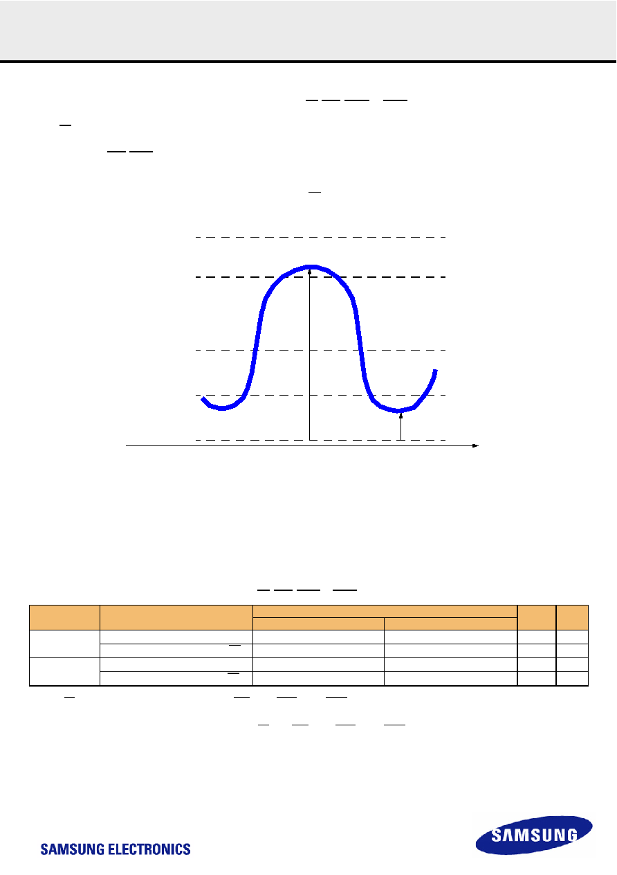
13.3.3 Single-ended Requirements for Differential Signals
Each individual component of a differential signal (CK, DQS, DQSL, DQSU, CK, DQS, DQSL, or DQSU) has also to comply with certain requirements for
single-ended signals.
CK and CK have to approximately reach VSEHmin / VSELmax (approximately equal to the ac-levels ( VIH(AC) / VIL(AC) ) for ADD/CMD signals) in every
half-cycle.
DQS, DQSL, DQSU, DQS, DQSL have to reach VSEHmin / VSELmax (approximately the ac-levels ( VIH(AC) / VIL(AC) ) for DQ signals) in every half-cycle
proceeding and following a valid transition.
Note that the applicable ac-levels for ADD/CMD and DQ’s might be different per speed-bin etc. E.g. if VIH150(AC)/VIL150(AC) is used for ADD/CMD
signals, then these ac-levels apply also for the single-ended signals CK and CK .
Figure 3. Single-ended requirement for differential signals
Note that while ADD/CMD and DQ signal requirements are with respect to VREF, the single-ended components of differential signals have a requirement
with respect to VDD/2; this is nominally the same. The transition of single-ended signals through the ac-levels is used to measure setup time. For single-
ended components of differential signals the requirement to reach VSELmax, VSEHmin has no bearing on timing, but adds a restriction on the common
mode characteristics of these signals.
[ Table 5 ] Single ended levels for CK, DQS, DQSL, DQSU, CK, DQS, DQSL or DQSU
NOTE :
1. For CK, CK use VIH/VIL(AC) of ADD/CMD; for strobes (DQS, DQS, DQSL, DQSL, DQSU, DQSU) use VIH/VIL(AC) of DQs.
2. VIH(AC)/VIL(AC) for DQs is based on VREFDQ; VIH(AC)/VIL(AC) for ADD/CMD is based on VREFCA; if a reduced ac-high or ac-low level is used for a signal group, then the
reduced level applies also here
3. These values are not defined, however the single-ended signals CK, CK, DQS, DQS, DQSL, DQSL, DQSU, DQSU need to be within the respective limits (VIH(DC) max,
VIL(DC)min) for single-ended signals as well as the limitations for overshoot and undershoot. Refer to "Overshoot and Undershoot Specification"
Symbol
Parameter
DDR3-800/1066/1333/1600
Unit
NOTE
Min
Max
VSEH
Single-ended high-level for strobes
(VDD/2)+0.175
NOTE 3
V
1, 2
Single-ended high-level for CK, CK
(VDD/2)+0.175
NOTE 3
V
1, 2
VSEL
Single-ended low-level for strobes
NOTE 3
(VDD/2)-0.175
V1, 2
Single-ended low-level for CK, CK
NOTE 3
(VDD/2)-0.175
V1, 2
VDD or VDDQ
VSEH min
VDD/2 or VDDQ/2
VSEL max
VSEH
VSS or VSSQ
VSEL
CK or DQS
time
相关PDF资料 |
PDF描述 |
|---|---|
| M393B5773CH0-CK0 | 256M X 72 MULTI DEVICE DRAM MODULE, 0.225 ns, DMA240 |
| M3950/1529A012 | TOGGLE SWITCH, 3PDT, LATCHED, 4A, 28VDC, THROUGH HOLE-STRAIGHT |
| M83731/2327D110 | TOGGLE SWITCH, 3PDT, MOMENTARY, 4A, 28VDC, THROUGH HOLE-STRAIGHT |
| M3950/1726A110 | TOGGLE SWITCH, 3PDT, LATCHED, 4A, 28VDC, THROUGH HOLE-STRAIGHT |
| M3E-R21ZQXFREQ | CRYSTAL OSCILLATOR, CLOCK, 1.5 MHz - 155.52 MHz, PECL OUTPUT |
相关代理商/技术参数 |
参数描述 |
|---|---|
| M393B5273CH0-CK004 | 制造商:Samsung 功能描述:4GBYTE REGISTERED DIMM, DDR3-1600 - Trays |
| M393B5273DH-CH9E8 | 制造商:Samsung Semiconductor 功能描述:4GB 2RX8 PC3-8500R-07-00-B0-D1 - Trays |
| M393B5670EH1 | 制造商:SAMSUNG 制造商全称:Samsung semiconductor 功能描述:DDR3 SDRAM Memory |
| M393B5670EH1-CF801 | 制造商:Samsung Semiconductor 功能描述:2GB DDR3 REGISTERED DIMM, 1066MHZ, - Trays |
| M393B5670EH1-CH904 | 制造商:Samsung Semiconductor 功能描述:2GBYTE REGISTERED DIMM,DDR3-1333 - Trays |
发布紧急采购,3分钟左右您将得到回复。