- 您现在的位置:买卖IC网 > PDF目录180205 > M393B5273CH0-CK0 512M X 72 MULTI DEVICE DRAM MODULE, 0.225 ns, DMA240 PDF资料下载
参数资料
| 型号: | M393B5273CH0-CK0 |
| 元件分类: | DRAM |
| 英文描述: | 512M X 72 MULTI DEVICE DRAM MODULE, 0.225 ns, DMA240 |
| 封装: | HALOGEN FREE AND ROHS COMPLIANT, DIMM-240 |
| 文件页数: | 57/58页 |
| 文件大小: | 1982K |
| 代理商: | M393B5273CH0-CK0 |
第1页第2页第3页第4页第5页第6页第7页第8页第9页第10页第11页第12页第13页第14页第15页第16页第17页第18页第19页第20页第21页第22页第23页第24页第25页第26页第27页第28页第29页第30页第31页第32页第33页第34页第35页第36页第37页第38页第39页第40页第41页第42页第43页第44页第45页第46页第47页第48页第49页第50页第51页第52页第53页第54页第55页第56页当前第57页第58页
datasheet
DDR3 SDRAM
Rev. 1.0
Registered DIMM
- 8 -
7. Input/Output Functional Description
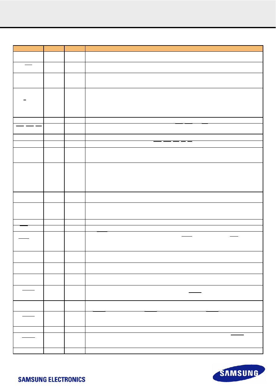
Symbol
Type
Polarity
Function
CK0
Input
Positive
Edge
Positive line of the differential pair of system clock inputs that drives input to the on-DIMM Clock Driver.
CK0
Input
Negative
Edge
Negative line of the differential pair of system clock inputs that drives the input to the on-DIMM Clock Driver.
CKE[1:0]
Input
Active High
CKE HIGH activates, and CKE LOW deactivates internal clock signals, and device input buffers
and output drivers of the SDRAMs. Taking CKE LOW provides PRECHARGE POWER-DOWN
and SELF REFRESH operation (all banks idle), or ACTIVE POWER DOWN (row ACTIVE in any bank)
S[3:0]
Input
Active Low
Enables the associated SDRAM command decoder when low and disables decoder when high.
When decoder is disabled, new commands are ignored and previous operations continue.
These input signals also disable all outputs (except CKE and ODT) of the register(s) on the DIMM when both
inputs are high. When both S[1:0] are high, all register outputs (except CKE, ODT and Chip select) remain in
the previous state. For modules supporting 4 ranks, S[3:2] operate similarly to S[1:0] for a second set of reg-
ister outputs.
ODT[1:0]
Input
Active High On-Die Termination control signals
RAS, CAS, WE
Input
Active Low
When sampled at the positive rising edge of the clock, CAS, RAS, and WE define the operation to be exe-
cuted by the SDRAM.
VREFDQ
Supply
Reference voltage for DQ0-DQ63 and CB0-CB7
VREFCA
Supply
Reference voltage for A0-A15, BA0-BA2, RAS, CAS, WE, S0, S1, CKE0, CKE1, Par_In, ODT0 and ODT1.
BA[2:0]
Input
Selects which SDRAM bank of eight is activated.
BA0 - BA2 define to which bank an Active, Read, Write or Precharge command is being applied. Bank
address also determines mode register is to be accessed during an MRS cycle.
A[15:13,
12/BC,11,
10/AP,9:0]
Input
Provided the row address for Active commands and the column address and Auto Precharge bit for Read/
Write commands to select one location out of the memory array in the respective bank. A10 is sampled dur-
ing a Precharge command to determine whether the Precharge applies to one bank (A10 LOW) or all banks
(A10 HIGH). If only one bank is to be precharged, the bank is selected by BA. A12 is also utilized for BL 4/8
identification for "BL on the fly" during CAS command. The address inputs also provide the op-code during
Mode Register Set commands.
DQ[63:0],
CB[7:0]
I/O
Data and Check Bit Input/Output pins
DM[8:0]
Active High Masks write data when high, issued concurrently with input data.
VDD, VSS Supply Power and ground for the DDR SDRAM input buffers and core logic.
VTT Supply Termination Voltage for Address/Command/Control/Clock nets.
DQS[17:0]
I/O
Positive Edge Positive line of the differential data strobe for input and output data.
DQS[17:0]
I/O
Negative Edge Negative line of the differential data strobe for input and output data.
TDQS[17:9],
TDQS[17:9]
OUT
TDQS/TDQS is applicable for X8 DRAMs only. When enabled via Mode Register A11=1 in MR1, DRAM will
enable the same termination resistance function on TDQS/TDQS that is applied to DQS/DQS. When dis-
abled via mode register A11=0 in MR1, DM/TDQS will provide the data mask function and TDQS is not used.
X4/X16 DRAMs must disable the TDQS function via mode register A11=0 in MR1
SA[2:0]
IN
These signals are tied at the system planar to either VSS or VDDSPD to configure the serial SPD EEPROM
address range.
SDA
I/O
This bidirectional pin is used to transfer data into or out of the SPD EEPROM. A resistor must be
connected from the SDA bus line to VDDSPD on the system planar to act as a pull-up.
SCL
IN
This signal is used to clock data into and out of the SPD EEPROM. A resistor may be connected
from the SCL bus time to VDDSPD on the system planar to act as a pull-up.
EVENT
OUT
(open
drain)
Active Low
This signal indicates that a thermal event has been detected in the thermal sensing device.The system
should guarantee the electrical level requirement is met for the EVENT pin on TS/SPD part.
VDDSPD
Supply
Serial EEPROM positive power supply wired to a separate power pin at the connector which supports from
3.0 Volt to 3.6 Volt (nominal 3.3V) operation.
RESET
IN
The RESET pin is connected to the RESET pin on the register and to the RESET pin on the DRAM. When
low, all register outputs will be driven low and the Clock Driver clocks to the DRAMs and register(s) will be set
to low level (the Clock Driver will remain synchronized with the input clock)
Par_In
IN
Parity bit for the Address and Control bus. ("1 " : Odd, "0 ": Even)
Err_Out
OUT
(open
drain)
Parity error detected on the Address and Control bus. A resistor may be connected from Err_Out
bus line to VDD on the system planar to act as a pull up.
TEST
Used by memory bus analysis tools (unused (NC) on memory DIMMs)
相关PDF资料 |
PDF描述 |
|---|---|
| M393B5773CH0-CK0 | 256M X 72 MULTI DEVICE DRAM MODULE, 0.225 ns, DMA240 |
| M3950/1529A012 | TOGGLE SWITCH, 3PDT, LATCHED, 4A, 28VDC, THROUGH HOLE-STRAIGHT |
| M83731/2327D110 | TOGGLE SWITCH, 3PDT, MOMENTARY, 4A, 28VDC, THROUGH HOLE-STRAIGHT |
| M3950/1726A110 | TOGGLE SWITCH, 3PDT, LATCHED, 4A, 28VDC, THROUGH HOLE-STRAIGHT |
| M3E-R21ZQXFREQ | CRYSTAL OSCILLATOR, CLOCK, 1.5 MHz - 155.52 MHz, PECL OUTPUT |
相关代理商/技术参数 |
参数描述 |
|---|---|
| M393B5273CH0-CK004 | 制造商:Samsung 功能描述:4GBYTE REGISTERED DIMM, DDR3-1600 - Trays |
| M393B5273DH-CH9E8 | 制造商:Samsung Semiconductor 功能描述:4GB 2RX8 PC3-8500R-07-00-B0-D1 - Trays |
| M393B5670EH1 | 制造商:SAMSUNG 制造商全称:Samsung semiconductor 功能描述:DDR3 SDRAM Memory |
| M393B5670EH1-CF801 | 制造商:Samsung Semiconductor 功能描述:2GB DDR3 REGISTERED DIMM, 1066MHZ, - Trays |
| M393B5670EH1-CH904 | 制造商:Samsung Semiconductor 功能描述:2GBYTE REGISTERED DIMM,DDR3-1333 - Trays |
发布紧急采购,3分钟左右您将得到回复。