- 您现在的位置:买卖IC网 > PDF目录180205 > M393B5273CH0-CK0 512M X 72 MULTI DEVICE DRAM MODULE, 0.225 ns, DMA240 PDF资料下载
参数资料
| 型号: | M393B5273CH0-CK0 |
| 元件分类: | DRAM |
| 英文描述: | 512M X 72 MULTI DEVICE DRAM MODULE, 0.225 ns, DMA240 |
| 封装: | HALOGEN FREE AND ROHS COMPLIANT, DIMM-240 |
| 文件页数: | 24/58页 |
| 文件大小: | 1982K |
| 代理商: | M393B5273CH0-CK0 |
第1页第2页第3页第4页第5页第6页第7页第8页第9页第10页第11页第12页第13页第14页第15页第16页第17页第18页第19页第20页第21页第22页第23页当前第24页第25页第26页第27页第28页第29页第30页第31页第32页第33页第34页第35页第36页第37页第38页第39页第40页第41页第42页第43页第44页第45页第46页第47页第48页第49页第50页第51页第52页第53页第54页第55页第56页第57页第58页
- 24 -
datasheet
DDR3 SDRAM
Rev. 1.0
Registered DIMM
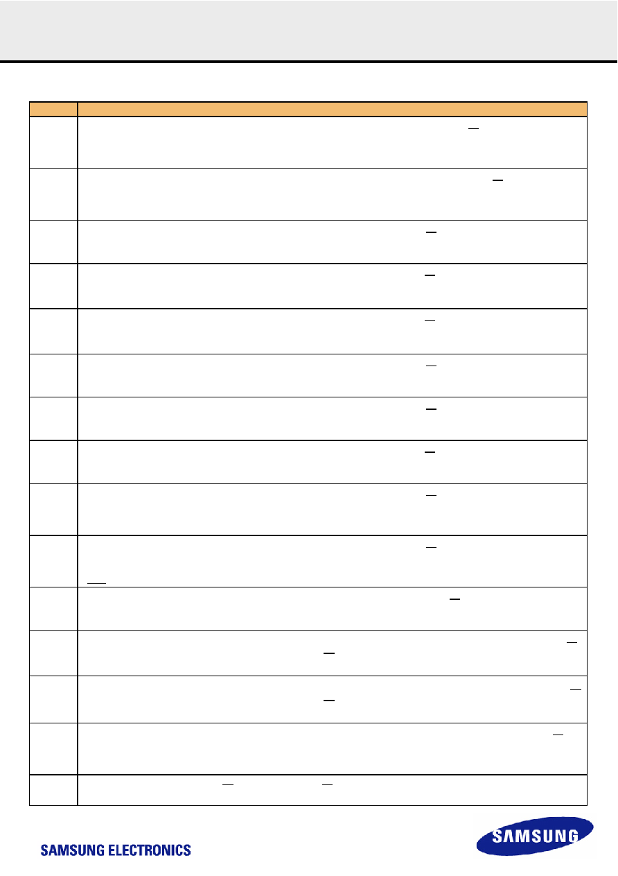
15. DIMM IDD specification definition
Symbol
Description
IDD0
Operating One Bank Active-Precharge Current
CKE: High; External clock: On; tCK, nRC, nRAS, CL: Refer to Component Datasheet for detail pattern ; BL: 81); AL: 0; CS: High between ACT and PRE;
Command, Address, Bank Address Inputs: partially toggling ; Data IO: FLOATING; DM:stable at 0; Bank Activity: Cycling with one bank active at a time:
0,0,1,1,2,2,... ; Output Buffer and RTT: Enabled in Mode Registers2); ODT Signal: stable at 0; Pattern Details: Refer to Component Datasheet for detail pat-
tern
IDD1
Operating One Bank Active-Read-Precharge Current
CKE: High; External clock: On; tCK, nRC, nRAS, nRCD, CL: Refer to Component Datasheet for detail pattern ; BL: 81); AL: 0; CS: High between ACT, RD
and PRE; Command, Address, Bank Address Inputs, Data IO: partially toggling ; DM:stable at 0; Bank Activity: Cycling with one bank active at a time:
0,0,1,1,2,2,... ; Output Buffer and RTT: Enabled in Mode Registers2); ODT Signal: stable at 0; Pattern Details: Refer to Component Datasheet for detail pat-
tern
IDD2N
Precharge Standby Current
CKE: High; External clock: On; tCK, CL: Refer to Component Datasheet for detail pattern ; BL: 81); AL: 0; CS: stable at 1; Command, Address, Bank
Address Inputs: partially toggling ; Data IO: FLOATING; DM:stable at 0; Bank Activity: all banks closed; Output Buffer and RTT: Enabled in Mode
Registers2); ODT Signal: stable at 0; Pattern Details: Refer to Component Datasheet for detail pattern
IDD2P0
Precharge Power-Down Current Slow Exit
CKE: Low; External clock: On; tCK, CL: Refer to Component Datasheet for detail pattern ; BL: 81); AL: 0; CS: stable at 1; Command, Address, Bank
Address Inputs: stable at 0; Data IO: FLOATING; DM:stable at 0; Bank Activity: all banks closed; Output Buffer and RTT: Enabled in Mode Registers2);
ODT Signal: stable at 0; Precharge Power Down Mode: Slow Exit3)
IDD2P1
Precharge Power-Down Current Fast Exit
CKE: Low; External clock: On; tCK, CL: Refer to Component Datasheet for detail pattern ; BL: 81); AL: 0; CS: stable at 1; Command, Address, Bank
Address Inputs: stable at 0; Data IO: FLOATING; DM:stable at 0; Bank Activity: all banks closed; Output Buffer and RTT: Enabled in Mode Registers2);
ODT Signal: stable at 0; Precharge Power Down Mode: Fast Exit3)
IDD2Q
Precharge Quiet Standby Current
CKE: High; External clock: On; tCK, CL: Refer to Component Datasheet for detail pattern ; BL: 81); AL: 0; CS: stable at 1; Command, Address, Bank
Address Inputs: stable at 0; Data IO: FLOATING; DM:stable at 0;Bank Activity: all banks closed; Output Buffer and RTT: Enabled in Mode Registers2);
ODT Signal: stable at 0
IDD3N
Active Standby Current
CKE: High; External clock: On; tCK, CL: Refer to Component Datasheet for detail pattern ; BL: 81); AL: 0; CS: stable at 1; Command, Address, Bank
Address Inputs: partially toggling ; Data IO: FLOATING; DM:stable at 0;Bank Activity: all banks open; Output Buffer and RTT: Enabled in Mode
Registers2); ODT Signal: stable at 0; Pattern Details: Refer to Component Datasheet for detail pattern
IDD3P
Active Power-Down Current
CKE: Low; External clock: On; tCK, CL: Refer to Component Datasheet for detail pattern ; BL: 81); AL: 0; CS: stable at 1; Command, Address, Bank
Address Inputs: stable at 0; Data IO: FLOATING;DM:stable at 0; Bank Activity: all banks open; Output Buffer and RTT: Enabled in Mode Registers2); ODT
Signal: stable at 0
IDD4R
Operating Burst Read Current
CKE: High; External clock: On; tCK, CL: Refer to Component Datasheet for detail pattern ; BL: 81); AL: 0; CS: High between RD; Command, Address,
Bank Address Inputs: partially toggling ; Data IO: seamless read data burst with different data between one burst and the next one ; DM:stable at 0; Bank
Activity: all banks open, RD commands cycling through banks: 0,0,1,1,2,2,... ; Output Buffer and RTT: Enabled in Mode Registers2); ODT Signal: stable
at 0; Pattern Details: Refer to Component Datasheet for detail pattern
IDD4W
Operating Burst Write Current
CKE: High; External clock: On; tCK, CL: Refer to Component Datasheet for detail pattern ; BL: 81); AL: 0; CS: High between WR; Command, Address,
Bank Address Inputs: partially toggling ; Data IO: seamless write data burst with different data between one burst and the next one ; DM: stable at 0; Bank
Activity: all banks open, WR commands cycling through banks: 0,0,1,1,2,2,... ; Output Buffer and RTT: Enabled in Mode Registers2); ODT Signal: stable
at HIGH; Pattern Details: Refer to Component Datasheet for detail pattern
IDD5B
Burst Refresh Current
CKE: High; External clock: On; tCK, CL, nRFC: Refer to Component Datasheet for detail pattern ; BL: 81); AL: 0; CS: High between REF; Command,
Address, Bank Address Inputs: partially toggling ; Data IO: FLOATING;DM:stable at 0; Bank Activity: REF command every nRFC ; Output Buffer and
RTT: Enabled in Mode Registers2); ODT Signal: stable at 0; Pattern Details: Refer to Component Datasheet for detail pattern
IDD6
Self Refresh Current: Normal Temperature Range
TCASE: 0 - 85°C; Auto Self-Refresh (ASR): Disabled4); Self-Refresh Temperature Range (SRT): Normal5); CKE: Low; External clock: Off; CK and CK:
LOW; CL: Refer to Component Datasheet for detail pattern ; BL: 81); AL: 0; CS, Command, Address, Bank Address, Data IO: FLOATING;DM:stable at 0;
Bank Activity: Self-Refresh operation; Output Buffer and RTT: Enabled in Mode Registers2); ODT Signal: FLOATING
IDD6ET
Self-Refresh Current: Extended Temperature Range (optional)6)
TCASE: 0 - 95°C; Auto Self-Refresh (ASR): Disabled4); Self-Refresh Temperature Range (SRT): Extended5); CKE: Low; External clock: Off; CK and CK:
LOW; CL: Refer to Component Datasheet for detail pattern ; BL: 81); AL: 0; CS, Command, Address, Bank Address, Data IO: FLOATING;DM:stable at 0;
Bank Activity: Extended Temperature Self-Refresh operation; Output Buffer and RTT: Enabled in Mode Registers2); ODT Signal: FLOATING
IDD7
Operating Bank Interleave Read Current
CKE: High; External clock: On; tCK, nRC, nRAS, nRCD, nRRD, nFAW, CL: Refer to Component Datasheet for detail pattern ; BL: 81); AL: CL-1; CS: High
between ACT and RDA; Command, Address, Bank Address Inputs: partially toggling ; Data IO: read data bursts with different data between one burst and
the next one ; DM:stable at 0; Bank Activity: two times interleaved cycling through banks (0, 1, ...7) with different addressing ; Output Buffer and RTT:
Enabled in Mode Registers2); ODT Signal: stable at 0; Pattern Details: Refer to Component Datasheet for detail pattern
IDD8
RESET Low Current
RESET : Low; External clock : off; CK and CK : LOW; CKE : FLOATING ; CS, Command, Address, Bank Address, Data IO : FLOATING ; ODT Signal :
FLOATING
相关PDF资料 |
PDF描述 |
|---|---|
| M393B5773CH0-CK0 | 256M X 72 MULTI DEVICE DRAM MODULE, 0.225 ns, DMA240 |
| M3950/1529A012 | TOGGLE SWITCH, 3PDT, LATCHED, 4A, 28VDC, THROUGH HOLE-STRAIGHT |
| M83731/2327D110 | TOGGLE SWITCH, 3PDT, MOMENTARY, 4A, 28VDC, THROUGH HOLE-STRAIGHT |
| M3950/1726A110 | TOGGLE SWITCH, 3PDT, LATCHED, 4A, 28VDC, THROUGH HOLE-STRAIGHT |
| M3E-R21ZQXFREQ | CRYSTAL OSCILLATOR, CLOCK, 1.5 MHz - 155.52 MHz, PECL OUTPUT |
相关代理商/技术参数 |
参数描述 |
|---|---|
| M393B5273CH0-CK004 | 制造商:Samsung 功能描述:4GBYTE REGISTERED DIMM, DDR3-1600 - Trays |
| M393B5273DH-CH9E8 | 制造商:Samsung Semiconductor 功能描述:4GB 2RX8 PC3-8500R-07-00-B0-D1 - Trays |
| M393B5670EH1 | 制造商:SAMSUNG 制造商全称:Samsung semiconductor 功能描述:DDR3 SDRAM Memory |
| M393B5670EH1-CF801 | 制造商:Samsung Semiconductor 功能描述:2GB DDR3 REGISTERED DIMM, 1066MHZ, - Trays |
| M393B5670EH1-CH904 | 制造商:Samsung Semiconductor 功能描述:2GBYTE REGISTERED DIMM,DDR3-1333 - Trays |
发布紧急采购,3分钟左右您将得到回复。