- 您现在的位置:买卖IC网 > PDF目录359091 > M68HC12B (飞思卡尔半导体(中国)有限公司) Microcontrollers PDF资料下载
参数资料
| 型号: | M68HC12B |
| 厂商: | 飞思卡尔半导体(中国)有限公司 |
| 英文描述: | Microcontrollers |
| 中文描述: | 微控制器 |
| 文件页数: | 169/334页 |
| 文件大小: | 1671K |
| 代理商: | M68HC12B |
第1页第2页第3页第4页第5页第6页第7页第8页第9页第10页第11页第12页第13页第14页第15页第16页第17页第18页第19页第20页第21页第22页第23页第24页第25页第26页第27页第28页第29页第30页第31页第32页第33页第34页第35页第36页第37页第38页第39页第40页第41页第42页第43页第44页第45页第46页第47页第48页第49页第50页第51页第52页第53页第54页第55页第56页第57页第58页第59页第60页第61页第62页第63页第64页第65页第66页第67页第68页第69页第70页第71页第72页第73页第74页第75页第76页第77页第78页第79页第80页第81页第82页第83页第84页第85页第86页第87页第88页第89页第90页第91页第92页第93页第94页第95页第96页第97页第98页第99页第100页第101页第102页第103页第104页第105页第106页第107页第108页第109页第110页第111页第112页第113页第114页第115页第116页第117页第118页第119页第120页第121页第122页第123页第124页第125页第126页第127页第128页第129页第130页第131页第132页第133页第134页第135页第136页第137页第138页第139页第140页第141页第142页第143页第144页第145页第146页第147页第148页第149页第150页第151页第152页第153页第154页第155页第156页第157页第158页第159页第160页第161页第162页第163页第164页第165页第166页第167页第168页当前第169页第170页第171页第172页第173页第174页第175页第176页第177页第178页第179页第180页第181页第182页第183页第184页第185页第186页第187页第188页第189页第190页第191页第192页第193页第194页第195页第196页第197页第198页第199页第200页第201页第202页第203页第204页第205页第206页第207页第208页第209页第210页第211页第212页第213页第214页第215页第216页第217页第218页第219页第220页第221页第222页第223页第224页第225页第226页第227页第228页第229页第230页第231页第232页第233页第234页第235页第236页第237页第238页第239页第240页第241页第242页第243页第244页第245页第246页第247页第248页第249页第250页第251页第252页第253页第254页第255页第256页第257页第258页第259页第260页第261页第262页第263页第264页第265页第266页第267页第268页第269页第270页第271页第272页第273页第274页第275页第276页第277页第278页第279页第280页第281页第282页第283页第284页第285页第286页第287页第288页第289页第290页第291页第292页第293页第294页第295页第296页第297页第298页第299页第300页第301页第302页第303页第304页第305页第306页第307页第308页第309页第310页第311页第312页第313页第314页第315页第316页第317页第318页第319页第320页第321页第322页第323页第324页第325页第326页第327页第328页第329页第330页第331页第332页第333页第334页
Timer Registers
M68HC12B Family Data Sheet, Rev. 9.1
Freescale Semiconductor
169
TSWAI — Timer Module Stops While in Wait Bit
TSWAI also affects pulse accumulators and modulus down counters.
0 = Allows the timer module to continue running during wait
1 = Disables the timer module when the MCU is in wait mode. Timer interrupts cannot be used to
get the MCU out of wait.
TSBCK — Timer and Modulus Counter Stop While in Background Mode Bit
TBSCK does not stop the pulse accumulator.
0 = Allows the timer and modulus counter to continue running while in background mode
1 = Disables the timer and modulus counter whenever the MCU is in background mode. This is
useful for emulation.
TFFCA — Timer Fast Flag Clear All Bit
0 = Allows the timer flag clearing to function normally
1 = For TFLG1($8E), a read from an input capture or a write to the output compare channel
($90–$9F) causes the corresponding channel flag, CnF, to be cleared. For TFLG2 ($8F), any
access to the TCNT register ($84, $85) clears the TOF flag. Any access to the PACN3 and
PACN2 registers ($A2, $A3) clears the PAOVF and PAIF flags in the PAFLG register ($A1).
Any access to the PACN1 and PACN0 registers ($A4, $A5) clears the PBOVF flag in the
PBFLG register ($B1). This has the advantage of eliminating software overhead in a separate
clear sequence. Extra care is required to avoid accidental flag clearing due to unintended
accesses.
13.4.7 Timer Control Registers
Read: Anytime
Write: Anytime
OMn Bits — Output Mode
OLn Bits — Output Level
These eight pairs of control bits are encoded to specify the output action to be taken as a result of a
successful OCn compare (see
Table 13-1
). When either OMn or OLn is 1, the pin associated with OCn
becomes an output tied to OCn regardless of the state of the associated DDRT bit.
NOTE
To enable output action by OMn and OLn bits on the timer port, the
corresponding bit in OC7M should be cleared.
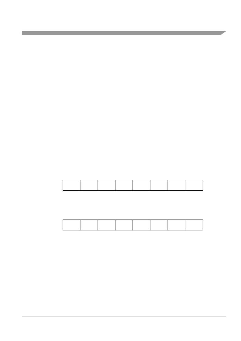
Address: $0088
Bit 7
6
5
4
3
2
1
Bit 0
Read:
Write:
Reset:
OM7
OL7
OM6
OL6
OM5
OL5
OM4
OL4
0
0
0
0
0
0
0
0
Figure 13-12. Timer Control Register 1 (TCTL1)
Address: $0089
Bit 7
6
5
4
3
2
1
Bit 0
Read:
Write:
Reset:
OM3
OL3
OM2
OL2
OM1
OL1
OM0
OL0
0
0
0
0
0
0
0
0
Figure 13-13. Timer Control Register 2 (TCTL2)
相关PDF资料 |
PDF描述 |
|---|---|
| M68HC705UGANG | High-density complementary metal oxide semiconductor (HCMOS) microcontroller unit |
| M68TC11E20B56 | HC11 Microcontrollers |
| M68Z128W-70N1T | 3V, 1 Mbit 128Kb x8 Low Power SRAM with Output Enable |
| M68Z128WN | 3V, 1 Mbit 128Kb x8 Low Power SRAM with Output Enable |
| M68Z128W | 3V, 1 Mbit 128Kb x8 Low Power SRAM with Output Enable |
相关代理商/技术参数 |
参数描述 |
|---|---|
| M68HC16Y1CFC | 制造商:MOTOROLA 制造商全称:Motorola, Inc 功能描述:16-Bit Modular Microcontroller |
| M68HC705UGANG | 制造商:FREESCALE 制造商全称:Freescale Semiconductor, Inc 功能描述:High-density complementary metal oxide semiconductor (HCMOS) microcontroller unit |
| M68HC705UPGMR | 制造商:FREESCALE 制造商全称:Freescale Semiconductor, Inc 功能描述:High-density complementary metal oxide semiconductor (HCMOS) microcontroller unit |
| M68HC705X16PGMR | 制造商:Rochester Electronics LLC 功能描述:- Bulk |
| M68HC711CFD | 制造商:MOTOROLA 制造商全称:Motorola, Inc 功能描述:CONFIG REGISTER PROGRAMMING FOR EEPROM-BASED MHC MICROCONTROLLERS |
发布紧急采购,3分钟左右您将得到回复。