- 您现在的位置:买卖IC网 > PDF目录67985 > MCIMX534AVV8C (FREESCALE SEMICONDUCTOR INC) 32-BIT, 800 MHz, RISC PROCESSOR, PBGA529 PDF资料下载
参数资料
| 型号: | MCIMX534AVV8C |
| 厂商: | FREESCALE SEMICONDUCTOR INC |
| 元件分类: | 微控制器/微处理器 |
| 英文描述: | 32-BIT, 800 MHz, RISC PROCESSOR, PBGA529 |
| 封装: | 19 X 19 MM, 0.80 MM PITCH, ROHS COMPLIANT, PLASTIC, TEPBGA-529 |
| 文件页数: | 101/178页 |
| 文件大小: | 4711K |
| 代理商: | MCIMX534AVV8C |
第1页第2页第3页第4页第5页第6页第7页第8页第9页第10页第11页第12页第13页第14页第15页第16页第17页第18页第19页第20页第21页第22页第23页第24页第25页第26页第27页第28页第29页第30页第31页第32页第33页第34页第35页第36页第37页第38页第39页第40页第41页第42页第43页第44页第45页第46页第47页第48页第49页第50页第51页第52页第53页第54页第55页第56页第57页第58页第59页第60页第61页第62页第63页第64页第65页第66页第67页第68页第69页第70页第71页第72页第73页第74页第75页第76页第77页第78页第79页第80页第81页第82页第83页第84页第85页第86页第87页第88页第89页第90页第91页第92页第93页第94页第95页第96页第97页第98页第99页第100页当前第101页第102页第103页第104页第105页第106页第107页第108页第109页第110页第111页第112页第113页第114页第115页第116页第117页第118页第119页第120页第121页第122页第123页第124页第125页第126页第127页第128页第129页第130页第131页第132页第133页第134页第135页第136页第137页第138页第139页第140页第141页第142页第143页第144页第145页第146页第147页第148页第149页第150页第151页第152页第153页第154页第155页第156页第157页第158页第159页第160页第161页第162页第163页第164页第165页第166页第167页第168页第169页第170页第171页第172页第173页第174页第175页第176页第177页第178页
Electrical Characteristics
i.MX53xA Automotive and Infotainment Applications Processors, Rev. 3
Freescale Semiconductor
29
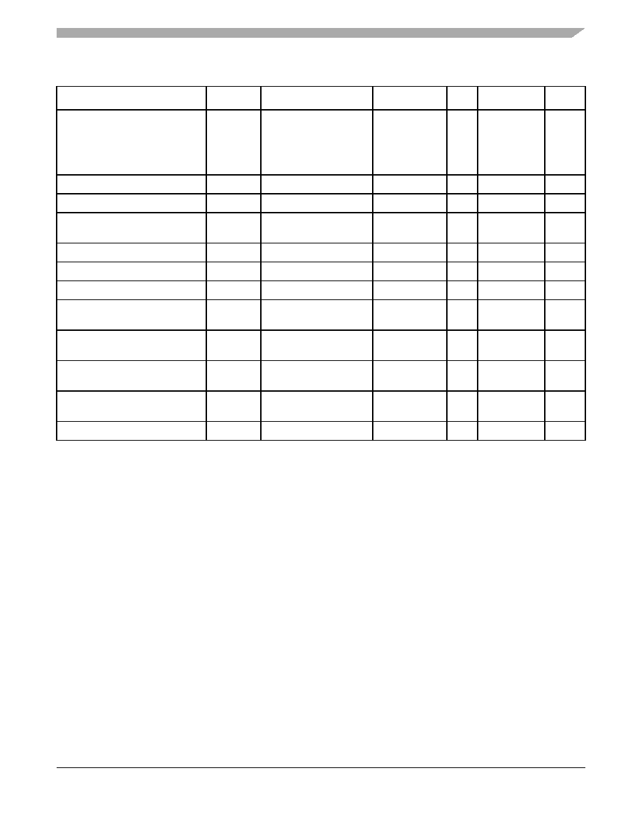
4.3.2
LPDDR2 I/O DC Parameters
The LPDDR2 I/O pads support DDR2/LVDDR2, LPDDR2, and DDR3 operational modes.
4.3.2.1
DDR2 Mode I/O DC Parameters
The DDR2 interface fully complies with JESD79-2E DDR2 JEDEC standard release April, 2008. The
Low-level output current
(1.65-3.1V OVDD)
Iol
Vout = 0.2
×OVDD
Low drive
Medium drive
High drive
Max drive
2.1
4.2
6.3
8.4
——
mA
High-Level DC input voltage1, 2
VIH
—
0.7
× OVDD
—
OVDD
V
Low-Level DC input voltage1, 2
VIL
—
0
—
0.3
× OVDD
V
Input Hysteresis
VHYS
OVDD = 1.875 V
OVDD = 2.775 V
0.25
0.34
0.45
—V
Schmitt trigger VT+2, 3
VT+
—
0.5
× OVDD
—
V
Schmitt trigger VT–2, 3
VT–
—
0.5
× OVDD
V
Input current (no pull-up/down)
Iin
Vin = OVDD or 0
—
2
μA
Input current (22 k
Ω Pull-up)
Iin
Vin = 0 V
Vin = OVDD
——
161
2
μA
Input current (47 k
Ω Pull-up)
Iin
Vin = 0 V
Vin = OVDD
——
76
2
μA
Input current (100 k
Ω Pull-up)
Iin
Vin = 0 V
Vin= OVDD
——
36
2
μA
Input current (100 k
Ω Pull-down)
Iin
Vin = 0 V
Vin = OVDD
——
2
36
μA
Keeper Circuit Resistance
—
1304
—k
Ω
1 Overshoot and undershoot conditions (transitions above OVDD and below GND) on switching pads must be held below 0.6 V,
and the duration of the overshoot/undershoot must not exceed 10% of the system clock cycle. Overshoot/ undershoot must be
controlled through printed circuit board layout, transmission line impedance matching, signal line termination, or other
methods. Non-compliance to this specification may affect device reliability or cause permanent damage to the device.
2 To maintain a valid level, the transition edge of the input must sustain a constant slew rate (monotonic) from the current DC
level through to the target DC level, VIL or VIH. Monotonic input transition time is from 0.1 ns to 1 s.
3 Hysteresis of 250 mV is guaranteed over all operating conditions when hysteresis is enabled.
4 Use an off-chip pull resistor of less than 60 k
Ω to override this keeper.
Table 10. GPIO I/O DC Electrical Characteristics (continued)
Parameter
Symbol
Test Conditions
Min
Typ
Max
Unit
相关PDF资料 |
PDF描述 |
|---|---|
| MCP23008T-E/SO | 8 I/O, PIA-GENERAL PURPOSE, PDSO18 |
| MCP23008-E/ML | 8 I/O, PIA-GENERAL PURPOSE, PQCC20 |
| MCP23S08T-E/ML | 8 I/O, PIA-GENERAL PURPOSE, PQCC20 |
| MCP23S08T-E/SS | 8 I/O, PIA-GENERAL PURPOSE, PDSO20 |
| MCP23008-E/P | 8 I/O, PIA-GENERAL PURPOSE, PDIP18 |
相关代理商/技术参数 |
参数描述 |
|---|---|
| MCIMX534AVV8C | 制造商:Freescale Semiconductor 功能描述:IC 32-BIT MPU 800 MHZ 529-BGA |
| MCIMX534AVV8CR2 | 功能描述:处理器 - 专门应用 iMX53 Rev 2.1 Auto RoHS:否 制造商:Freescale Semiconductor 类型:Multimedia Applications 核心:ARM Cortex A9 处理器系列:i.MX6 数据总线宽度:32 bit 最大时钟频率:1 GHz 指令/数据缓存: 数据 RAM 大小:128 KB 数据 ROM 大小: 工作电源电压: 最大工作温度:+ 95 C 安装风格:SMD/SMT 封装 / 箱体:MAPBGA-432 |
| MCIMX535DVV1B | 功能描述:处理器 - 专门应用 IMX53 REV 2.0 COMM RoHS:否 制造商:Freescale Semiconductor 类型:Multimedia Applications 核心:ARM Cortex A9 处理器系列:i.MX6 数据总线宽度:32 bit 最大时钟频率:1 GHz 指令/数据缓存: 数据 RAM 大小:128 KB 数据 ROM 大小: 工作电源电压: 最大工作温度:+ 95 C 安装风格:SMD/SMT 封装 / 箱体:MAPBGA-432 |
| MCIMX535DVV1C | 功能描述:处理器 - 专门应用 IMX53 REV 2.1 COMM RoHS:否 制造商:Freescale Semiconductor 类型:Multimedia Applications 核心:ARM Cortex A9 处理器系列:i.MX6 数据总线宽度:32 bit 最大时钟频率:1 GHz 指令/数据缓存: 数据 RAM 大小:128 KB 数据 ROM 大小: 工作电源电压: 最大工作温度:+ 95 C 安装风格:SMD/SMT 封装 / 箱体:MAPBGA-432 |
| MCIMX535DVV1C | 制造商:Freescale Semiconductor 功能描述:IMX53 REV 2.1 COMM |
发布紧急采购,3分钟左右您将得到回复。