- 您现在的位置:买卖IC网 > PDF目录67985 > MCIMX534AVV8C (FREESCALE SEMICONDUCTOR INC) 32-BIT, 800 MHz, RISC PROCESSOR, PBGA529 PDF资料下载
参数资料
| 型号: | MCIMX534AVV8C |
| 厂商: | FREESCALE SEMICONDUCTOR INC |
| 元件分类: | 微控制器/微处理器 |
| 英文描述: | 32-BIT, 800 MHz, RISC PROCESSOR, PBGA529 |
| 封装: | 19 X 19 MM, 0.80 MM PITCH, ROHS COMPLIANT, PLASTIC, TEPBGA-529 |
| 文件页数: | 16/178页 |
| 文件大小: | 4711K |
| 代理商: | MCIMX534AVV8C |
第1页第2页第3页第4页第5页第6页第7页第8页第9页第10页第11页第12页第13页第14页第15页当前第16页第17页第18页第19页第20页第21页第22页第23页第24页第25页第26页第27页第28页第29页第30页第31页第32页第33页第34页第35页第36页第37页第38页第39页第40页第41页第42页第43页第44页第45页第46页第47页第48页第49页第50页第51页第52页第53页第54页第55页第56页第57页第58页第59页第60页第61页第62页第63页第64页第65页第66页第67页第68页第69页第70页第71页第72页第73页第74页第75页第76页第77页第78页第79页第80页第81页第82页第83页第84页第85页第86页第87页第88页第89页第90页第91页第92页第93页第94页第95页第96页第97页第98页第99页第100页第101页第102页第103页第104页第105页第106页第107页第108页第109页第110页第111页第112页第113页第114页第115页第116页第117页第118页第119页第120页第121页第122页第123页第124页第125页第126页第127页第128页第129页第130页第131页第132页第133页第134页第135页第136页第137页第138页第139页第140页第141页第142页第143页第144页第145页第146页第147页第148页第149页第150页第151页第152页第153页第154页第155页第156页第157页第158页第159页第160页第161页第162页第163页第164页第165页第166页第167页第168页第169页第170页第171页第172页第173页第174页第175页第176页第177页第178页
i.MX53xA Automotive and Infotainment Applications Processors, Rev. 3
112
Freescale Semiconductor
Electrical Characteristics
4.7.13
PATA Timing Parameters
This section describes the timing parameters of the Parallel ATA module which are compliant with
ATA/ATAPI-6 specification.
Parallel ATA module can work on PIO/Multi-Word DMA/Ultra DMA transfer modes. Each transfer mode
has different data transfer rate, Ultra DMA mode 4 data transfer rate is up to 100MB/s. Parallel ATA
module interface consist of a total of 29 pins. Some pins act on different function in different transfer
mode. There are different requirements of timing relationships among the function pins conform with
ATA/ATAPI-6 specification and these requirements are configurable by the ATA module registers.
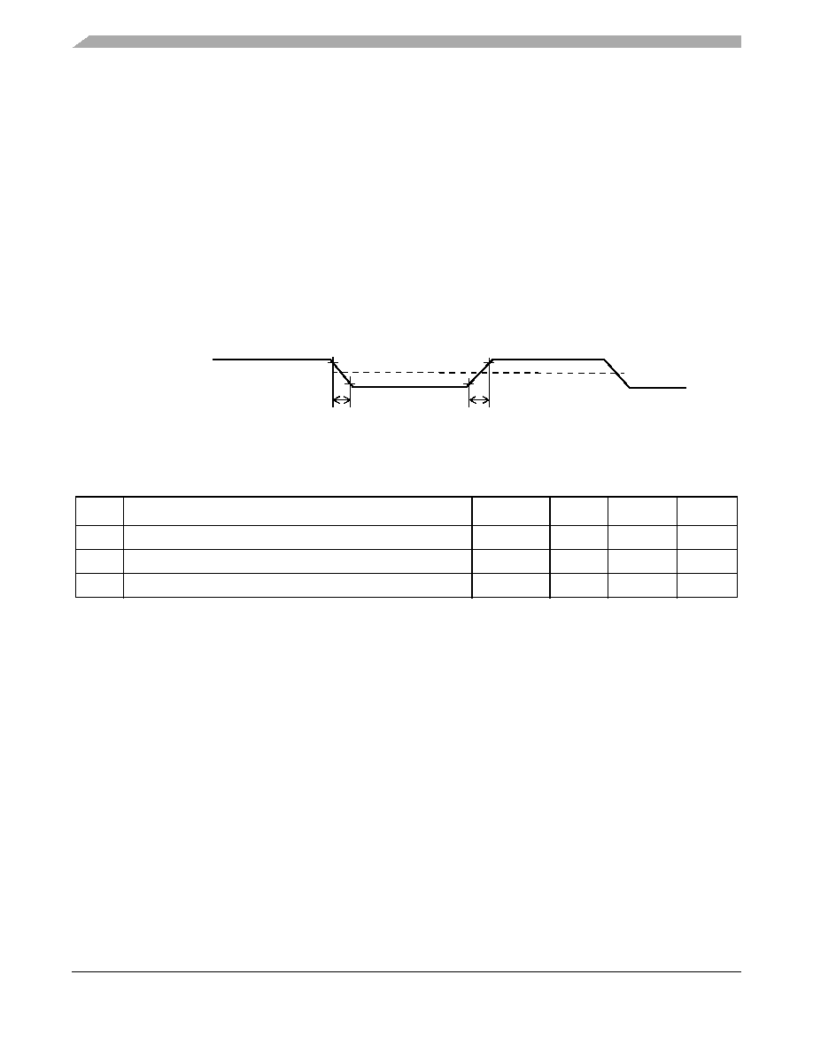
Table 71 and Figure 65 define the AC characteristics of all the PATA interface signals in all data transfer
modes.
Figure 65. PATA Interface Signals Timing Diagram
The user must use level shifters for 5.0 V compatibility on the ATA interface. The i.MX53xA PATA
interface is 3.3 V compatible.
The use of bus buffers introduces delay on the bus and skew between signal lines. These factors make it
difficult to operate the bus at the highest speed (UDMA-5) when bus buffers are used. If fast UDMA mode
operation is needed, this may not be compatible with bus buffers.
Another area of attention is the slew rate limit imposed by the ATA specification on the ATA bus.
According to this limit, any signal driven on the bus should have a slew rate between 0.4 and 1.2 V/ns with
a 40 pF load. Not many vendors of bus buffers specify slew rate of the outgoing signals.
When bus buffers are used, the ata_data bus buffer is special. This is a bidirectional bus buffer, so a
direction control signal is needed. This direction control signal is ata_buffer_en. When its high, the bus
should drive from host to device. When its low, the bus should drive from device to host. Steering of the
signal is such that contention on the host and device tri-state busses is always avoided.
Table 71. AC Characteristics of All Interface Signals
ID
Parameter
Symbol
Min
Max
Unit
SI1
Rising edge slew rate for any signal on ATA interface1
1 SRISE and SFALL shall meet this requirement when measured at the sender’s connector from 10–90% of full signal
amplitude with all capacitive loads from 15
–40 pF where all signals have the same capacitive load value.
Srise
—1.25
V/ns
SI2
Falling edge slew rate for any signal on ATA interface1
Sfall
—1.25
V/ns
SI3
Host interface signal capacitance at the host connector
Chost
—20
pF
ATA Interface Signals
SI1
SI2
相关PDF资料 |
PDF描述 |
|---|---|
| MCP23008T-E/SO | 8 I/O, PIA-GENERAL PURPOSE, PDSO18 |
| MCP23008-E/ML | 8 I/O, PIA-GENERAL PURPOSE, PQCC20 |
| MCP23S08T-E/ML | 8 I/O, PIA-GENERAL PURPOSE, PQCC20 |
| MCP23S08T-E/SS | 8 I/O, PIA-GENERAL PURPOSE, PDSO20 |
| MCP23008-E/P | 8 I/O, PIA-GENERAL PURPOSE, PDIP18 |
相关代理商/技术参数 |
参数描述 |
|---|---|
| MCIMX534AVV8C | 制造商:Freescale Semiconductor 功能描述:IC 32-BIT MPU 800 MHZ 529-BGA |
| MCIMX534AVV8CR2 | 功能描述:处理器 - 专门应用 iMX53 Rev 2.1 Auto RoHS:否 制造商:Freescale Semiconductor 类型:Multimedia Applications 核心:ARM Cortex A9 处理器系列:i.MX6 数据总线宽度:32 bit 最大时钟频率:1 GHz 指令/数据缓存: 数据 RAM 大小:128 KB 数据 ROM 大小: 工作电源电压: 最大工作温度:+ 95 C 安装风格:SMD/SMT 封装 / 箱体:MAPBGA-432 |
| MCIMX535DVV1B | 功能描述:处理器 - 专门应用 IMX53 REV 2.0 COMM RoHS:否 制造商:Freescale Semiconductor 类型:Multimedia Applications 核心:ARM Cortex A9 处理器系列:i.MX6 数据总线宽度:32 bit 最大时钟频率:1 GHz 指令/数据缓存: 数据 RAM 大小:128 KB 数据 ROM 大小: 工作电源电压: 最大工作温度:+ 95 C 安装风格:SMD/SMT 封装 / 箱体:MAPBGA-432 |
| MCIMX535DVV1C | 功能描述:处理器 - 专门应用 IMX53 REV 2.1 COMM RoHS:否 制造商:Freescale Semiconductor 类型:Multimedia Applications 核心:ARM Cortex A9 处理器系列:i.MX6 数据总线宽度:32 bit 最大时钟频率:1 GHz 指令/数据缓存: 数据 RAM 大小:128 KB 数据 ROM 大小: 工作电源电压: 最大工作温度:+ 95 C 安装风格:SMD/SMT 封装 / 箱体:MAPBGA-432 |
| MCIMX535DVV1C | 制造商:Freescale Semiconductor 功能描述:IMX53 REV 2.1 COMM |
发布紧急采购,3分钟左右您将得到回复。