- 您现在的位置:买卖IC网 > PDF目录67985 > MCIMX534AVV8C (FREESCALE SEMICONDUCTOR INC) 32-BIT, 800 MHz, RISC PROCESSOR, PBGA529 PDF资料下载
参数资料
| 型号: | MCIMX534AVV8C |
| 厂商: | FREESCALE SEMICONDUCTOR INC |
| 元件分类: | 微控制器/微处理器 |
| 英文描述: | 32-BIT, 800 MHz, RISC PROCESSOR, PBGA529 |
| 封装: | 19 X 19 MM, 0.80 MM PITCH, ROHS COMPLIANT, PLASTIC, TEPBGA-529 |
| 文件页数: | 121/178页 |
| 文件大小: | 4711K |
| 代理商: | MCIMX534AVV8C |
第1页第2页第3页第4页第5页第6页第7页第8页第9页第10页第11页第12页第13页第14页第15页第16页第17页第18页第19页第20页第21页第22页第23页第24页第25页第26页第27页第28页第29页第30页第31页第32页第33页第34页第35页第36页第37页第38页第39页第40页第41页第42页第43页第44页第45页第46页第47页第48页第49页第50页第51页第52页第53页第54页第55页第56页第57页第58页第59页第60页第61页第62页第63页第64页第65页第66页第67页第68页第69页第70页第71页第72页第73页第74页第75页第76页第77页第78页第79页第80页第81页第82页第83页第84页第85页第86页第87页第88页第89页第90页第91页第92页第93页第94页第95页第96页第97页第98页第99页第100页第101页第102页第103页第104页第105页第106页第107页第108页第109页第110页第111页第112页第113页第114页第115页第116页第117页第118页第119页第120页当前第121页第122页第123页第124页第125页第126页第127页第128页第129页第130页第131页第132页第133页第134页第135页第136页第137页第138页第139页第140页第141页第142页第143页第144页第145页第146页第147页第148页第149页第150页第151页第152页第153页第154页第155页第156页第157页第158页第159页第160页第161页第162页第163页第164页第165页第166页第167页第168页第169页第170页第171页第172页第173页第174页第175页第176页第177页第178页
Electrical Characteristics
i.MX53xA Automotive and Infotainment Applications Processors, Rev. 3
Freescale Semiconductor
47
4.6.5
NAND Flash Controller (NFC) Parameters
This section provides the relative timing requirements among various signals of NFC at the module level,
in each operational mode.
Timing parameters in Figure 10, Figure 11, Figure 12, Figure 13, Figure 15, and Table 35 show the default
NFC mode (asymmetric mode) using two Flash clock cycles per one access of RE_B and WE_B.
Timing parameters in Figure 10, Figure 11, Figure 12, Figure 14, Figure 15, and Table 35 show symmetric
NFC mode using one Flash clock cycle per one access of RE_B and WE_B.
With reference to the timing diagrams, a high is defined as 80% of signal value and low is defined as 20%
of signal value. All parameters are given in nanoseconds. The BGA contact load used in calculations is
20 pF (except for NF16 - 40 pF) and there is maximum drive strength on all contacts.
All timing parameters are a function of T, which is the period of the flash_clk clock (“enfc_clk” at system
level). This clock frequency can be controlled by the user, configuring CCM (SoC clock controller). The
clock is derived from emi_slow_clk after single divider.
Figure 34 demonstrates several examples of clock frequency settings.
NOTE
A potential limitation for minimum clock frequency may exist for some
devices. When the clock frequency is too low, the data bus capturing might
occur after the specified trhoh (RE_B high to output hold) period. Setting the
clock frequency above 25.6 MHz (that is, T = 39 ns) guaranties a proper
operation for devices having trhoh > 15 ns. It is also recommended that the
NFC_FREQ_SEL Fuse be set accordingly to initiate the boot with
33.33 MHz clock.
4 T
dpdref is the time period of the reference clock after predivider. According to the specification, the maximum lock time in FOL
mode is 398 cycles of divided reference clock when DPLL starts after full reset.
5 Tdck is the time period of the output clock, dpdck_2.
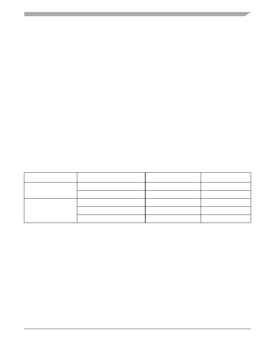
Table 34. NFC Clock Settings Examples
emi_slow_clk (MHz)
nfc_podf (Division Factor)
enfc_clk (MHz)
T-Clock Period (ns)
100 (Boot mode)
71
1 Boot value NFC_FREQ_SEL Fuse High (burned)
14.29
70
32
2 Boot value NFC_FREQ_SEL Fuse Low
33.33
30
133
4
33.33
30
3
44.333
3 For RBB_MODE=1, using NANDF_RB0 signal for ready/busy indication. This mode require setting the delay line. See the
Reference Manual for details.
22.5
2663
15
相关PDF资料 |
PDF描述 |
|---|---|
| MCP23008T-E/SO | 8 I/O, PIA-GENERAL PURPOSE, PDSO18 |
| MCP23008-E/ML | 8 I/O, PIA-GENERAL PURPOSE, PQCC20 |
| MCP23S08T-E/ML | 8 I/O, PIA-GENERAL PURPOSE, PQCC20 |
| MCP23S08T-E/SS | 8 I/O, PIA-GENERAL PURPOSE, PDSO20 |
| MCP23008-E/P | 8 I/O, PIA-GENERAL PURPOSE, PDIP18 |
相关代理商/技术参数 |
参数描述 |
|---|---|
| MCIMX534AVV8C | 制造商:Freescale Semiconductor 功能描述:IC 32-BIT MPU 800 MHZ 529-BGA |
| MCIMX534AVV8CR2 | 功能描述:处理器 - 专门应用 iMX53 Rev 2.1 Auto RoHS:否 制造商:Freescale Semiconductor 类型:Multimedia Applications 核心:ARM Cortex A9 处理器系列:i.MX6 数据总线宽度:32 bit 最大时钟频率:1 GHz 指令/数据缓存: 数据 RAM 大小:128 KB 数据 ROM 大小: 工作电源电压: 最大工作温度:+ 95 C 安装风格:SMD/SMT 封装 / 箱体:MAPBGA-432 |
| MCIMX535DVV1B | 功能描述:处理器 - 专门应用 IMX53 REV 2.0 COMM RoHS:否 制造商:Freescale Semiconductor 类型:Multimedia Applications 核心:ARM Cortex A9 处理器系列:i.MX6 数据总线宽度:32 bit 最大时钟频率:1 GHz 指令/数据缓存: 数据 RAM 大小:128 KB 数据 ROM 大小: 工作电源电压: 最大工作温度:+ 95 C 安装风格:SMD/SMT 封装 / 箱体:MAPBGA-432 |
| MCIMX535DVV1C | 功能描述:处理器 - 专门应用 IMX53 REV 2.1 COMM RoHS:否 制造商:Freescale Semiconductor 类型:Multimedia Applications 核心:ARM Cortex A9 处理器系列:i.MX6 数据总线宽度:32 bit 最大时钟频率:1 GHz 指令/数据缓存: 数据 RAM 大小:128 KB 数据 ROM 大小: 工作电源电压: 最大工作温度:+ 95 C 安装风格:SMD/SMT 封装 / 箱体:MAPBGA-432 |
| MCIMX535DVV1C | 制造商:Freescale Semiconductor 功能描述:IMX53 REV 2.1 COMM |
发布紧急采购,3分钟左右您将得到回复。