- 您现在的位置:买卖IC网 > PDF目录67985 > MCIMX534AVV8C (FREESCALE SEMICONDUCTOR INC) 32-BIT, 800 MHz, RISC PROCESSOR, PBGA529 PDF资料下载
参数资料
| 型号: | MCIMX534AVV8C |
| 厂商: | FREESCALE SEMICONDUCTOR INC |
| 元件分类: | 微控制器/微处理器 |
| 英文描述: | 32-BIT, 800 MHz, RISC PROCESSOR, PBGA529 |
| 封装: | 19 X 19 MM, 0.80 MM PITCH, ROHS COMPLIANT, PLASTIC, TEPBGA-529 |
| 文件页数: | 93/178页 |
| 文件大小: | 4711K |
| 代理商: | MCIMX534AVV8C |
第1页第2页第3页第4页第5页第6页第7页第8页第9页第10页第11页第12页第13页第14页第15页第16页第17页第18页第19页第20页第21页第22页第23页第24页第25页第26页第27页第28页第29页第30页第31页第32页第33页第34页第35页第36页第37页第38页第39页第40页第41页第42页第43页第44页第45页第46页第47页第48页第49页第50页第51页第52页第53页第54页第55页第56页第57页第58页第59页第60页第61页第62页第63页第64页第65页第66页第67页第68页第69页第70页第71页第72页第73页第74页第75页第76页第77页第78页第79页第80页第81页第82页第83页第84页第85页第86页第87页第88页第89页第90页第91页第92页当前第93页第94页第95页第96页第97页第98页第99页第100页第101页第102页第103页第104页第105页第106页第107页第108页第109页第110页第111页第112页第113页第114页第115页第116页第117页第118页第119页第120页第121页第122页第123页第124页第125页第126页第127页第128页第129页第130页第131页第132页第133页第134页第135页第136页第137页第138页第139页第140页第141页第142页第143页第144页第145页第146页第147页第148页第149页第150页第151页第152页第153页第154页第155页第156页第157页第158页第159页第160页第161页第162页第163页第164页第165页第166页第167页第168页第169页第170页第171页第172页第173页第174页第175页第176页第177页第178页
Electrical Characteristics
i.MX53xA Automotive and Infotainment Applications Processors, Rev. 3
Freescale Semiconductor
21
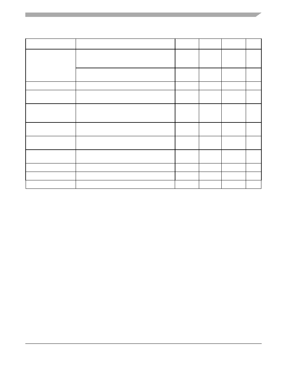
TVDAC_DHVDD7
TVDAC_AHVDDRGB7
TVE digital and analog power supply, TVE-to-DAC
level shifter supply, cable detector supply, analog
power supply to RGB channel
2.69
2.75
2.91
V
For GPIO use only, when TVE is not in use
1.65
1.8 or
2.775
3.1
V
NVCC_SRTC_POW
SRTC Core and slow I/O Supply (GPIO)8
1.25
1.3
1.35
V
NVCC_RESET
LVIO
1.65
1.8 or
2.775
3.1
V
USB_H1_VDDA25
USB_OTG_VDDA25
NVCC_XTAL
USB_PHY analog supply, oscillator amplifier analog
supply9
2.25
2.5
2.75
V
USB_H1_VDDA33
USB_OTG_VDDA33
USB PHY I/O analog supply
3.0
3.3
3.6
V
VBUS
for details. Note that this is not a power supply.
——
—
VDD_REG10
Power supply input for the integrated linear
regulators
2.37
2.5
2.63
V
VP
SATA PHY core power supply
1.25
1.3
1.35
V
VPH
SATA PHY I/O supply voltage
2.25
2.5
2.75
V
TJ
Junction Temperature
–40
10511
125
oC
1 Voltage at the package power supply contact must be maintained between the minimum and maximum voltages. The design
must allow for supply tolerances and system voltage drops.
2 The nominal values for the supplies indicate the target setpoint for a tolerance no tighter than ± 50 mV. Use of supplies with a
tighter tolerance allows reduction of the setpoint with commensurate power savings.
3 VDDA and VDDAL1 can be driven by the VDD_DIG_PLL internal regulator using external connections. When operating in this
configuration, the regulator is still operating at the default 1.2 V, as bootup start. During bootup initialization, software should
increase this regulator voltage to match VCC (1.3 V nominal) in order to reduce internal leakage current.
4 By default, VDD_DIG_PLL is driven from internal on-die 1.2 V linear regulator (LDO). In this case, there is no need driving this
supply externally. LDO output to VDD_DIG_PLL should be configured by software after power-up to 1.3 V output. A bypass
capacitor of minimal value 22
μF should be connected to this pad in any case whether it is driven internally or externally. Use
of the on-chip LDO is preferred. See i.MX53 System Development User’s Guide.
5 By default, the VDD_ANA_PLL is driven from internal on-die 1.8 V linear regulator (LDO). In this case there is no need driving
this supply externally. A bypass capacitor of minimal value 22
μF should be connected to this pad in any case whether it is
driven internally or externally. Use of the on-chip LDO is preferred. See i.MX53 System Development User’s Guide.
6 After fuses are programmed, Freescale strongly recommends the best practice of reading the fuses to verify that they are
written correctly. In Read mode, VDD_FUSE should be floated or grounded. Tying VDD_FUSE to a positive supply (3.0 V–3.3
V) increases the possibility of inadvertently blowing fuses and is not recommended in read mode.
7 If not using TVE module or other pads in this power domain for the product, the TVDAC_DHVDD and TVDAC_AHVDDRGB
can remain floating.
8 GPIO pad operational at low frequency
9 The analog supplies should be isolated in the application design. Use of series inductors is recommended.
10 VDD_REG is power supply input for the integrated linear regulators of VDD_ANA_PLL and VDD_DIG_PLL when they are
configured to the internal supply option. VDDR_REG still has to be tied to 2.5 V supply when VDD_ANA_PLL and
VDD_DIG_PLL are configured for external power supply mode although in this case it is not used as supply source.
Table 6. i.MX53xA Operating Ranges (continued)
Symbol
Parameter
Minimum1 Nominal2 Maximum1
Unit
相关PDF资料 |
PDF描述 |
|---|---|
| MCP23008T-E/SO | 8 I/O, PIA-GENERAL PURPOSE, PDSO18 |
| MCP23008-E/ML | 8 I/O, PIA-GENERAL PURPOSE, PQCC20 |
| MCP23S08T-E/ML | 8 I/O, PIA-GENERAL PURPOSE, PQCC20 |
| MCP23S08T-E/SS | 8 I/O, PIA-GENERAL PURPOSE, PDSO20 |
| MCP23008-E/P | 8 I/O, PIA-GENERAL PURPOSE, PDIP18 |
相关代理商/技术参数 |
参数描述 |
|---|---|
| MCIMX534AVV8C | 制造商:Freescale Semiconductor 功能描述:IC 32-BIT MPU 800 MHZ 529-BGA |
| MCIMX534AVV8CR2 | 功能描述:处理器 - 专门应用 iMX53 Rev 2.1 Auto RoHS:否 制造商:Freescale Semiconductor 类型:Multimedia Applications 核心:ARM Cortex A9 处理器系列:i.MX6 数据总线宽度:32 bit 最大时钟频率:1 GHz 指令/数据缓存: 数据 RAM 大小:128 KB 数据 ROM 大小: 工作电源电压: 最大工作温度:+ 95 C 安装风格:SMD/SMT 封装 / 箱体:MAPBGA-432 |
| MCIMX535DVV1B | 功能描述:处理器 - 专门应用 IMX53 REV 2.0 COMM RoHS:否 制造商:Freescale Semiconductor 类型:Multimedia Applications 核心:ARM Cortex A9 处理器系列:i.MX6 数据总线宽度:32 bit 最大时钟频率:1 GHz 指令/数据缓存: 数据 RAM 大小:128 KB 数据 ROM 大小: 工作电源电压: 最大工作温度:+ 95 C 安装风格:SMD/SMT 封装 / 箱体:MAPBGA-432 |
| MCIMX535DVV1C | 功能描述:处理器 - 专门应用 IMX53 REV 2.1 COMM RoHS:否 制造商:Freescale Semiconductor 类型:Multimedia Applications 核心:ARM Cortex A9 处理器系列:i.MX6 数据总线宽度:32 bit 最大时钟频率:1 GHz 指令/数据缓存: 数据 RAM 大小:128 KB 数据 ROM 大小: 工作电源电压: 最大工作温度:+ 95 C 安装风格:SMD/SMT 封装 / 箱体:MAPBGA-432 |
| MCIMX535DVV1C | 制造商:Freescale Semiconductor 功能描述:IMX53 REV 2.1 COMM |
发布紧急采购,3分钟左右您将得到回复。